Download
1 / 16
160 likes | 303 Vues
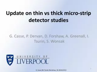
Update on thin vs thick micro-strip detector studies. G. Casse, P. Dervan, D. Forshaw, A. Greenall , I. Tsurin , S. Wonsak. CONTEXT:.

E N D
Update on thin vs thick micro-strip detector studies G. Casse, P. Dervan, D. Forshaw, A. Greenall, I. Tsurin, S. Wonsak G. Casse 8th Trento Workshop, 18-20/02/2013
CONTEXT: The choice of thin silicon sensors seems to meet the requirements for lowering the material budget of the vertex detectors, providing at the same time accrued radiation hardness (at very high doses). But, how thin can they be? This certainly depends on the application and the characteristics of the detector system. Microstrip detectors are not the configuration where reduced thickness can be pushed to the lower limits. Nonetheless studying the radiation hardness properties of thin microstrip sensors gives valuable indication on the change of their properties. We show here the CC(V) measurements of 50, 100, 140 and 300 mm thick after irradiation to doses of 2E16 neq cm-2. Irradiation with reactor neutrons performed at the JSI reactor, usual thanks to V. Cindro et al., prtonsMauric Glaser et al. G. Casse 8th Trento Workshop, 18-20/02/2013
The method Sensors made by Micron Semiconductor on 4” wafers with thicknesses 50, 100, 140, 300 mm. 1x1 cm2, 80 mm pitch, n-in-p devices. The 50 mm thick would break (mechanically) when attached to the cooling block due to the different CTE. No measurements available after irradiation (when cooling is needed). Analogue information from the Alibava board (equipped with Beetle chip) Mip signal from 90Sr source Irradiations performed in the JSI Ljubljana research nuclear reactor G. Casse 8th Trento Workshop, 18-20/02/2013
Measurements before irradiation Charge Collection vs Bias (CC(V)) for the 50, 100, 140, 300 mm un-irradiated sensors. As expected the signal varies linearly with thickness G. Casse 8th Trento Workshop, 18-20/02/2013
300µm Degradation of the CC(V) with neutron fluence for the 300mm thick sensors. G. Casse 8th Trento Workshop, 18-20/02/2013
140µm Degradation of the CC(V) with neutron fluence for the 140mm thick sensors. Likely mislabelling of one sensor, it looks like the irradiation dose of 5E15 neqcm-2 is missing. G. Casse 8th Trento Workshop, 18-20/02/2013
100µm Degradation of the CC(V) with neutron fluence for the 100mm thick sensors. Likely mislabelling of one sensor, it looks like the irradiation dose of 5E15 neqcm-2 is missing. G. Casse 8th Trento Workshop, 18-20/02/2013
2x10¹⁵neq cm-2 Comparison of the CC(V) after this dose for the 100, 140 and 300mm thick sensors. Collected charge similar at low voltages. G. Casse 8th Trento Workshop, 18-20/02/2013
1x10¹⁶neq cm-2 Comparison of the CC(V) after this dose for the 100, 140 and 300mm thick sensors. Thinner sensor exhibit better collected charge at same applied bias voltage. G. Casse 8th Trento Workshop, 18-20/02/2013
2x10¹⁶neq cm-2 Comparison of the CC(V) after this dose for the 100, 140 and 300mm thick sensors. Thinner sensor exhibit better collected charge at same applied bias voltage. G. Casse 8th Trento Workshop, 18-20/02/2013
Degradation 300µm G. Casse 8th Trento Workshop, 18-20/02/2013
Degradation 140µm CC(V) G. Casse 8th Trento Workshop, 18-20/02/2013
Degradation 100µm CC(V) G. Casse 8th Trento Workshop, 18-20/02/2013
Degradation 50µm CC(V) G. Casse 8th Trento Workshop, 18-20/02/2013
Degradation all thicknesses 600 V 1000 V G. Casse 8th Trento Workshop, 18-20/02/2013
CONCLUSIONS Thin sensors deliver higher charge collection than standard (300mm) silicon sensors after about 2E15 neq cm-2. The thinnest 50mm sensor exhibits no degradation of CCE between 0 to 2×10¹⁶neq cm-2. 100mm sensors also show an advantage towards the 140mm thick after the highest dose (2E15 neq cm-2). We should study a wider range of fluences with extremely thin devices.. It is also possible that fine thickness tuning is key for experiment application (65, 75mm thick devices should equally be studied). Mechanical reasons are also important in this respect. G. Casse 8th Trento Workshop, 18-20/02/2013