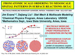
Atomic-Scale Manipulation of Spins in Nanomagnets for Advanced Information Technology
360 likes | 491 Vues
This study explores the engineering of spins at the atomic scale using STM techniques at the IBM Almaden Research Center. It highlights the significance of magnetism in data storage and novel computation methods that leverage magnetic properties. The research focuses on fabricating nanomagnets that emulate model spin systems and the detailed manipulation of individual magnetic atoms on surfaces. Techniques include spin excitation spectroscopy and electronic-structure calculations, showcasing the potential of atomic-scale spin engineering for future information technology applications.

Atomic-Scale Manipulation of Spins in Nanomagnets for Advanced Information Technology
E N D
Presentation Transcript
Atomic-scale Engeered Spins at a Surface Chiung-Yuan Lin IBM Almaden Research Center
Nanomagnetism and Information Technology • Magnetism is at the heart of data storage. • Many novel computations schemes are based on manipulation of magnetic properties. Courtesy of Hitachi J.R. Petta et al. Science309, 2180 (2005) A. Imre et al. Science311, 205 (2006)
Nanomagnets • Fabricated nanomagnets can recreate model spin systems such as spin ice. • A small number of atomic spins can be coupled in metal clusters or molecular magnetic structures. R.F. Wang et al., Nature439, 303 (2006) Fe8, courtesy ESF. M.B. Knickelbein Phys. Rev. B70, 14424 (2004)
|ST,m> |ST,m> |1,+1> |5/2,+5/2> |5/2,+3/2> |1,0> |5/2,+1/2> Energy Energy |5/2,-1/2> |1,-1> |5/2,-3/2> |5/2,-5/2> |0,0> Magnetic Field Magnetic Field STM Studies of Atomic-Scale Spin-Coupling • Manipulation on thin insulators:build individual nanomagnets with an STM • Spin Excitation Spectroscopy: collective spin excitations of individual nanostructures 10Mn chain Mn atom Science 312, 1021 (2006)
Keep it Simple: Free Mn Atom 4s • Half filled d-shell • Weak spin-orbit interactions 3d Mn: S = 5/2, L = 0, J = 5/2
dI/dV V 0 Scanning Tunneling Spectroscopy: LDOS Ef eV tip sample Features in the local DOS are reflected in dI/dV.
Thin insulating layer Magnetic Atoms on Surfaces Magnetic atom • Atom’s spin is screened by conduction electrons (Kondo effect) • A thin insulating layer may isolate the atomic spin Metal surface
Ef Ef eV D D eV X tip sample tip sample D D |eV| < D Elastic Channel Open Inelastic Channel Closed |eV| > D Elastic Channel Open Inelastic Channel Open Inelastic Electron Tunneling Spectroscopy Non-magnetic tip Thin insulator Magnetic atom dI/dV kBT < D σe+σie σe Non-magnetic sample eV -D D 0
Methods of Electronic-structure Calculation Plane wave Atomic spheres Atomic partial wave Atomic partial wave Interstitial region • Full-potential Linearized Augmented Plane Wave basis • Periodic-slab geometry (5-layer Cu + 8-layer vacuum) • Density Functional Theory Generalized Gradiant Approximation (GGA) PBE96: Perdew et al., PRL 77, 3865 (1996) • Structure Optimization
Methods of Electronic-structure Calculation Cu Cu Cu Cu vacuum vacuum vacuum • FLAPW basis • Periodic-slab geometry (5-layer Cu + 8-layer vacuum) • Density Functional Theory Generalized Gradiant Approximation (GGA) PBE96: Perdew et al., PRL 77, 3865 (1996) • Structure Optimization
Methods of Electronic-structure Calculation • FLAPW basis • Periodic-slab geometry (5-layer Cu + 8-layer vacuum) • Density Functional Theory Generalized Gradiant Approximation (GGA) PBE96: Perdew et al., PRL 77, 3865 (1996) • Structure Optimization
N a0=Ö2d0 Cu d0 Thin Insulator: CuN Islands on Cu(100) d0=2.55Å a0=3.60Å 1nm • Atomic resolution on CuN • Mn atoms bind to Cu and N sites CuN Mn Mn Mn Mn Mn Mn Cu(100) CuN monolayer Cu(100)
0.25Å 1.80Å DFT Calculation of Electron Density in CuN N atoms are approximately coplanar with Cu atoms on CuN surface. N-1 N-1 Cu+0.5 Cu+0.5 Cu+0.5 Cu Cu
Pick up Atom Manipulation of Mn on Cu(100) / CuN • Move tip in • Apply 2.0V • Pull tip back
Pick up Atom Drop off Manipulation of Mn on Cu(100) / CuN • Move tip in • Apply -0.5V • Pull tip back
N Cu Mn Mn Spectroscopy of Mn Dimers • Large step at ~6mV splits into three distinct steps at high fields
|ST,m> E |1,+1> |1,0> |1,-1> |0,0> B Coupled Spins 5 4 … 1 0 • S=5/2 Ä S=5/2 ST = • For ST=0 (singlet) the first excited state is ST=1 (triplet) • Three excitations around constant energy shift
IBM Almaden STM Lab has built chains of up to 10 Mn atoms on Cu binding sites Cu(100) 2 6 1nm 3 7 10Mn 1Mn 4 8 CuN 1nm 5 9 Mn Mn Mn Chains of Mn Atoms N Cu
2 6 1nm 3 7 4 8 5 9 Spectroscopy of Mn Chains 10 Spectra change dramatically with each additional Mn atom.
Heisenberg Model of Spin Coupling J S • Phenomenological Exchange Coupling • J = Coupling strength • Si = spin of ith atom • Assumptions • All spins are the same • Nearest-neighbor coupling • All J are the same • J > 0 (antiferromagnetic coupling)
Heisenberg Dimer Spectrum • SG=0 and SE=1 • Atomic spin affects numbers of levels but not spacing • First excited state at J J S
Determination of Spin Coupling Strength • From the dimer spectrum J=6.2meV • Variations in J of ±5% for different dimers at various locations J=6.2meV
Determination of Atomic Spin • Using J = 6.2meV, we find S=5/2 • STM determines both J and S! S=3 S=5/2 S=2 J=6.2meV
Heisenberg Model for Longer Chains • Use J = 6.2meV and S=5/2 • Odd chains • ground state spin = 5/2 • excited state spin = 3/2 • Even chains • ground state spin = 0 • excited state spin = 1
Unit Cells Used in Calculating Mn on CuN Single Mn, larger unit cell Single Mn, smallest unit cell Mn dimer, smallest unit cell N Cu Mn Mn 10.80Å 7.20Å 7.20Å
Electron Density with an Adsorbed Mn Atom Mn+ N -1.5 N -1.5 Cu+0.5 Cu+0.5 Cu Cu Cu • N atoms move farther out of surface Cu layer towards Mn atom. • Cu atom being pushed into the surface. • This “isolates” the free spin of Mn atom.
Mn Spin from DFT majority () minority () Free Mn atom 3d 5S=5/2
A new kind of atomic-scale magnet • Surface N atoms isolate and bridge Mn atoms. • This is a “surface” assembled magnet. Mn Mn N N N Cu Cu Cu Cu Cu
Control of Spin Coupling Strength J=6.2meV J=2.7meV STM can switch J by a factor of 2 by selecting the binding site
GGA+U GGA+U (strong Coulomb repulsion on Mn 3d) Calculating U by constraint GGA • Calculating U • Lock d-orbital into the atomic sphere • Do GGA for Mn d3 d2.5 and d3 d1.5 • U=Δεd of the above two
N Cu Calculating Exchange Coupling H=JS1·S2 |±|S=5/2, Sz=±5/2 DFT total energies = EE 2S2J=++|H|++ +-|H| +-
Calculating Exchange Coupling (in meV)
Summary of theoretical work • The nontrivial structure of the engineered spins requires DFT to determine. • Calculated structure shows a new kind of molecular magnets. • GGA+U produces correct S and very accurate J; very helpful for searching a system of desired S and J.
What’s Next • Can we understand IETS processes? • matrix elements, selection rules, transition strengths • What is the origin of the exchange coupling? • superexchange, delocalized electrons • Are other interactions possible? • vary distances, shapes, types of atoms • Can we control anisotropy effects? • Find a way to store and transfer spin information:bits and circuits based on atomic spins
Chris Lutz Andreas Heinrich Barbara Jones CyrusHirjibehedin Thanks to
