Download
1 / 18
200 likes | 601 Vues
Free-Space MEMS Tunable Optical Filter in (110) Silicon. Ariel Lipson & Eric M. Yeatman Optical & Semiconductor Group. Imperial College London. Optical & Semiconductor Devices - E.E.E. Dept. Outline. Device - Optical Filter Optical analysis Fabrication. Schematic. Fabricated.

E N D
Free-Space MEMS Tunable Optical Filter in (110) Silicon Ariel Lipson & Eric M. Yeatman Optical & Semiconductor Group Imperial CollegeLondon Optical & Semiconductor Devices - E.E.E. Dept.
Outline • Device - Optical Filter • Optical analysis • Fabrication Schematic Fabricated
Device Application Optical Communication Network Broadcast System Lasers Fibre 400 channels • Tunable receiver • Spectrometer • Sensor
Device Configuration • 1D Photonic band gapTwo alternating materials • Dimensions are in the order of ¼ of a wavelength (or odd multiples) • Multiple reflections and phase matching create a wavelengthselectivemirror • Two mirrors form a Fabry-Perot filter
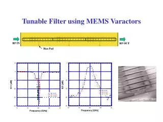
Lensed Fiber Lensed Fiber 200mm Device Configuration 150mm Air • 1D PBG structure3 silicon bar mirrors and a cavity – Fabry Perot • Dimensions~2mm thick x 25mm deep • Collimating Lensed fibers9mm radius Gaussian beam • Alignment grooves& springs created with an additional etch step • Tuning by varying the centre cavity width Light beam Oxide Silicon Alignment Springs Filter
r1,t1(l,f) nH nL f mair¼lc mgap½lc msi¼lc Optical Analysis The ideal case • Transfer matrix formulation • Mode overlap integralwith the exit fiber • Gaussian beam inputPlane wave expansion of Gaussian beam using spatial Fourier transform
Optical Analysis The ideal case • Collimation decreases losses • Layer thickness effects losses and pass band • Optical communication systems need narrow pass bands ~100GHz
J r1,t1(l,f) r2,t2(l,f) L01 Lp2 f Lp1 mair¼lc mgap½lc msi¼lc Optical Analysis The non-ideal case • Due to imperfect deep etching, angles are introduced • Fabry-Perot cavity analysis for a wedged cavity with a PBG mirror on either side
Optical Analysis The non-ideal case • Simulation for an 9mm Gaussian beam with different etching angles • Ripples appear at high frequencies • Above >0.001 deg we get excess loss and pass band widening vertical etching! Optics Letters 1st Feb 2006
Optical Analysis The non-ideal case • From “Principles of Optics” by Born and Wolf • Fizeau fringes…
DRIE followed by short KOH etching in (110) silicon: • Vertical etching • Smooth surfaces • If kept short, does not effect too much other orientations Fabrication • Deep Reactive Ion Etching (DRIE): • Suitable for all silicon orientations • Scalloping and 1-2° deg sidewall angle. • KOH etching in (110) silicon (Kendall 1979): • Vertical etching, but limited by etch ratio between (111):(110) • Smooth surfaces • Not suitable for non (111) planes • Depth limited by width and length
DRIE KOH wet etching Fabrication DRIE + KOH
Fabrication Process Flow 1. Dry Oxidation of a BSOI 5. DRIE – device layer 2. Back Etching 6. DRIE – handle layer Photo resist Oxide Silicon Gold 3. Device pattern 7. DRIE + KOH – device layer Fiber 4. Handle pattern 8. Release oxide
Fabrication Results – Static Filter • 0.65nm pass band, -10.5dB loss and a 200Ghz channel spacing • MEMS tuning mechanisms • <0.01° deg verticality
Fabrication Results – Tunable Filter • Back etching release works well. • Moving cantilevers 10mm
Fabrication Results – Tunable Filter Undercuts Stiction because of wet processing • KOH smoothing is far from ideal on BSOI. • Under cut because of notching problem in DRIE. • Additional loss due to lateral angles while tuning. Unsmooth surfaces Notching effect in DRIE
Summary • 1D PBG Static filter was fabricated for DWDM networks with -10.5 dB fiber to fiber losses, 200 GHz channel spacing. • Tunable filter but wide pass band. • Combined DRIE + KOH wet etching on (110) silicon wafers for very vertical (<0.01°) and smooth surfaces.
Acknowledgments • We would like to thank the UPC, Lambdax and Coventor for their support. • Thanks to Dr. John Stagg, Dr. Munir Ahmad and Michael Larsson for their kind help. Further information: alipson@ic.ac.uk