1 / 59

Ch 9. Memory, CPLDs, and FPGAs

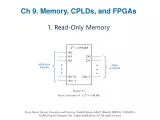
Ch 9. Memory, CPLDs, and FPGAs. 1. Read-Only Memory. Az : output polarity control Az = 0 output active low Az = 1 output active high. 9.1.1 Using ROMs for “Random” Combinational Logic Function. 9.1.1 Using ROMs for “Random” Combinational Logic Function.

trent
Télécharger la présentation

Ch 9. Memory, CPLDs, and FPGAs

An Image/Link below is provided (as is) to download presentation Download Policy: Content on the Website is provided to you AS IS for your information and personal use and may not be sold / licensed / shared on other websites without getting consent from its author. Content is provided to you AS IS for your information and personal use only. Download presentation by click this link. While downloading, if for some reason you are not able to download a presentation, the publisher may have deleted the file from their server. During download, if you can't get a presentation, the file might be deleted by the publisher.

E N D

Presentation Transcript


  1. Ch 9. Memory, CPLDs, and FPGAs 1. Read-Only Memory

  2. Az : output polarity control Az = 0 output active low Az = 1 output active high

  3. 9.1.1 Using ROMs for “Random” Combinational Logic Function

  4. 9.1.1 Using ROMs for “Random” Combinational Logic Function

  5. 9.1.1 Using ROMs for “Random” Combinational Logic Function

  6. 9.1.1 Using ROMs for “Random” Combinational Logic Function

  7. 9.1.1 Using ROMs for “Random” Combinational Logic Function

  8. 9.1.1 Using ROMs for “Random” Combinational Logic Function

  9. 9.1.2 Internal ROM Structure If diode present, 1 Otherwise, Ø

  10. 9.1.2 Internal ROM Structure Diodes are missing, then D3 – D0 = 0111 instead of 0010

  11. 9.1.3 Two-Dimensional Decoding To reduce decoding complexity -> 7 to 128 decoder is huge -> instead, 3 – to 8 decoder + 16 – to – 1 MUX

  12. 9.1.3 Two-Dimensional Decoding If tr exist, 1 Otherwise, Ø

  13. 9.1.3 Two-Dimensional Decoding

  14. 9.1.4 Commercial ROM Types

  15. 9.1.4 Commercial ROM Types

  16. 9.1.4 Commercial ROM Types

  17. 9.1.5 ROM Control Inputs and Timing Three state bus OE : output enable CS : chip select OE & CS must be assecped 32k x 8bit ROM x 4 = 128kbytes (= 215 x 4 = 217) 17address bits

  18. 9.1.5 ROM Control Inputs and Timing

  19. 9.1.5 ROM Control Inputs and Timing

  20. 9.1.6 ROM Applications

  21. 9.1.6 ROM Applications In many phone connections, your voice is purposely attennated by a few decibels to make things work better (page. 729)

  22. 9.1.6 ROM Applications

  23. 9.1.6 ROM Applications

  24. 9.1.6 ROM Applications

  25. 9.1.6 ROM Applications

  26. 3. Static RAM • 9.3.1 Static-RAM Inputs and Outputs

  27. 9.3.1 Static-RAM Inputs and Outputs D-latch when SEL = Ø OUT <- Q when SEL = WR = Ø D <- IN

  28. 9.3.2 Static-RAM Internal Structure

  29. 9.3.3 Static-RAM Timing

  30. 9.3.3 Static-RAM Timing

  31. 9.3.4 Standard Static-RAMs

  32. 9.3.4 Standard Static-RAMs

  33. 9.3.5 Synchronous SRAM

  34. 9.3.5 Synchronous SRAM

  35. 9.3.5 Synchronous SRAM

  36. 9.3.5 Synchronous SRAM

  37. 9.3.5 Synchronous SRAM

  38. 4. Dynamic RAM • 9.4.1 Dynamic-RAM Structure To store 1, word = bit = 1 To store Ø, word 1, bit = Ø Bit line prechanged between H&1 To read, word = H If cell = 1 Bit line = 1 If cell = Ø, bit line = Ø

  39. 9.4.1 Dynamic-RAM Structure

  40. 9.4.1 Dynamic-RAM Structure

  41. 9.4.1 Dynamic-RAM Structure

  42. 9.4.2 SDRAM Timing

  43. 9.4.2 SDRAM Timing

  44. 9.4.2 SDRAM Timing

  45. 9.4.2 SDRAM Timing

  46. 5. Complex Programmable Logic Devices

  47. 9.5.1 Xilinx XC9500 CPLD Family

  48. 9.5.1 Xilinx XC9500 CPLD Family

  49. 9.5.2 Function-Block Architecture

  50. 9.5.2 Function-Block Architecture

More Related