Download
1 / 9
150 likes | 415 Vues
Autonomous On-Wafer Sensor Arrays. SFR Workshop November 8, 1999 Mason Freed, Kameshwar Poolla, and Costas Spanos Berkeley, CA.

E N D
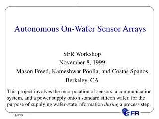
Autonomous On-Wafer Sensor Arrays SFR Workshop November 8, 1999 Mason Freed, Kameshwar Poolla, and Costas Spanos Berkeley, CA This project involves the incorporation of sensors, a communication system, and a power supply onto a standard silicon wafer, for the purpose of supplying wafer-state information during a process step.
Overview • Motivation • Certain wafer-state variables are difficult or destructive to measure, and many are impossible to measure in real-time • Add-on in-situ measurement devices are costly and cumbersome • Proposal: distributed sensor array on a wafer
I I Poly-Si V Test-Case: Etch Rate • Polysilicon etch rate sensors based on van der Pauw probe electrical film-thickness measurement: • Use wired connections for power and communications • Initial testing in XeF2, an isotropic, gaseous etchant • No problem making connections to wafer • No electrical or physical isolation necessary
Design #1 • Connections made using “edge-board” connector: Sensors Edge-board connector
Results (Design #1) • Eleven etch cycles performed, interferometric thickness measurements made between each cycle. • Repeatability: 12.89 Å • Accuracy: 45.9 Å • Stability: 3.2 Å drift in 15 minutes.
Design #2 Temperature-referenced Sensors Surface mount multiplexers Edge-board pads
Results (Design #2) • Preliminary test of a single sensor only, during etch
Progress vs Milestones Year 1 • Demonstrate tethered, real-time etch-rate measurements in chemical, non-plasma etch. (Done) Year 2 • Demonstrate un-tethered real-time measurements with integrated power and data processing. (Work in progress)
Future Work Next Year • Conduct testing of new sensor design. • Research isolation schemes to allow operation in plasma conditions. • Work on integrating power and communications modules onto sensor wafer, for wireless operation. 2000-2002 • Develop additional integrated sensors for plasma. • Develop sensors for other processes (DUV resist processing, Rapid Thermal Processing steps.)
![Self-Organization in Autonomous Sensor/Actuator Networks [SelfOrg]](https://cdn0.slideserve.com/962849/self-organization-in-autonomous-sensor-actuator-networks-selforg-dt.jpg)

![Self-Organization in Autonomous Sensor/Actuator Networks [ SelfOrg ]](https://cdn1.slideserve.com/2192758/self-organization-in-autonomous-sensor-actuator-networks-selforg-dt.jpg)
![Self-Organization in Autonomous Sensor/Actuator Networks [ SelfOrg ]](https://cdn1.slideserve.com/2361302/self-organization-in-autonomous-sensor-actuator-networks-selforg-dt.jpg)