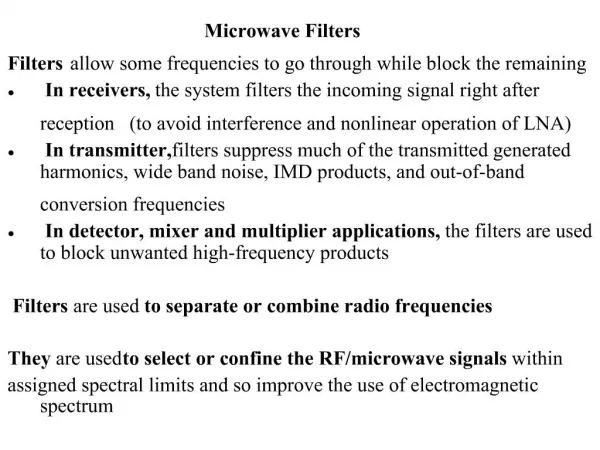
Recent Advances in Microwave Filters
590 likes | 936 Vues
Recent Advances in Microwave Filters. Professor Ian Hunter* CEng FIEEE FIET Institute of Microwaves and Photonics School of Electronic and Electrical Engineering University of Leeds * i.c.hunter@leeds.ac.uk. Outline. Frequency Selective Limiters Reconfigurable Filters

Recent Advances in Microwave Filters
E N D
Presentation Transcript
Recent Advances in Microwave Filters Professor Ian Hunter* CEng FIEEE FIET Institute of Microwaves and Photonics School of Electronic and Electrical Engineering University of Leeds *i.c.hunter@leeds.ac.uk
Outline • Frequency Selective Limiters • Reconfigurable Filters • Filter Techniques Applied to Antenna Design D. TunableBandstop Filters
A. Frequency Selective Limiter • Very desirable at the front end of wideband receivers for electronic warfare systems. • Benefits are to improve the receiver sensitivity, reduce signal’s dynamic range and increase probability of interception.
Nonlinear Bandstop Filters • Integration of a bandstop resonator and a schottky diode. • One module works for a particular frequency. They are cascaded for broadband operation. • This is a novel technique for a device called “Frequency Selective Limiter”
Г1= Г2= Г S11= 0 (all ω) S12= 0 (at ω0) S12= jГ (other ω) FSLs using Nonlinear Bandstop Filters • Simple nonlinear bandstop filters have relatively low Q. • Passive enhancement of resonator Q using reflection mode circuit. • Input and output ports are matched. • Bandstop response at ω0 when R=1 (matching condition). • Allpass response at other ω and when R≠ l (mismatch). At resonance with R=1:
First order Nonlinear Bandstop Filters (1) • A first order sub-network consists of one resonator and one schottky diode. • An impedance inverter (K) is used for impedance matching. • Lumped to microstrip circuit transformation using reactance slope parameter .
Multi-resonator Nonlinear Bandstop Filters (1) • The lowpass prototype will be subjected to frequency transformation and lumped to microstrip transformation.
Multi-resonator Nonlinear Bandstop Filters (2) Transfer response Reflection response Rise Time Fall Time Intermodulation Third order prototype
Multi-channel Nonlinear Bandstop Filters (2) CH 1 CH 2 CH 3 Prototype of a cascaded nonlinear bandstop filter
B. Reconfigurable Filters SDL Tunable Filter Switched Delay Line Resonator
Experimental Results Microstrip Prototype Cascaded 3-section Wilkinson Power Divider State-1 filter response: - D1 (Forward Bias) State-2 filter response: - D2 (Forward Bias) Scaled impedance U.E Z=4 • Rogers Duroid 6010 • Switch element : Infineon BAR50-02V in SC79 package.
Experimental Results S parameter Measurements • 2-state tuning from 1.06GHz to 1.51GHz ~35% tuning bandwidth. • Maximum passband loss of 1.7dB.
Experimental Results IP3 Measurements • Input power sweep - 0, 5 dBm • Frequency separation - 50kHz to 1000kHz • IP3>32dBm State 1 centered at 1.06GHz State 2 centered at 1.51GHz
Narrowband Quasi-Elliptic Filter Parallel-coupled SDL Filter
Narrowband Quasi-Elliptic Filter Parallel-coupled SDL Filter
Experimental Results Tunable Filter with Constant Bandwidth Cascaded 3-section Wilkinson Power Divider Impedance scaling • Rogers Duroid 6010 • Switch element : Infineon BAR50-02V in SC79 package.
Experimental Results S parameter Measurements • Three switched states with center frequency at 1, 1.3 and 1.6 GHz • Passband loss = 2.5- 4 dB • 45% tuning bandwidth • Constant bandwidth (50 MHz) tuning across the entire tuning range. • Immune from power saturation effect.
IP3 Measurements • Input power sweep - 0, 5 dBm • Frequency separation - 50kHz to 1000kHz • IP3>20dBm
Microstrip Antennas • A microstrip device is formed of two parallel conductors separated by a thin dielectric substrate (thickness<< λ) and the lower conductor acting as a ground plane. • Radiation relatively is broad beam broadside to the plane of the substrates, this type of antenna can be fabricated using photolithographic technique.
Microstrip Antennas • Advantages • Easy and low costs fabrications. • Strong mechanical structure and less weight. • Patch antennas are probably the most likely option to be integrated in microwave systems for their planner structure. • Disadvantages • Low efficiency. • Poor polarisation purity. • Narrow bandwidth.
Microstrip Antennas • Dominant Mode is the TM110 • Microstrip Antennas can be modelled as a high quality cavity resonator, that treat the side walls as Perfectly Magnetic Conductors while the top and bottom walls of the cavity are Perfectly Conducting Electric Walls. • Impedance is maximum at the edges and zero at the centre. • The radiation is the result of leakage from the cylindrical cavity, via the cavity laterals.
Filter Techniques Applied to Antenna Design • Dualmode Antenna; • Patch antennas, both square and circular, may support two orthogonal resonant modes. • Each of the resonant modes radiates and can be represented by a resonant circuit terminated by a resistor.
Filter Techniques Applied to Antenna Design • Theory • The fundamental resonant mode of this structure is the dual degenerate TM110 mode, where each of the resonant modes radiates and can be represented by a resonant circuit terminated in a resistor. • The equivalent circuit of dual mode patch antenna is a second ordered ladder network where each resonant circuit is terminated in a resistor R, representing its own internal losses and radiation.
S11(p) = Filter Techniques Applied to Antenna Design • Theory • The return loss of the equivalent circuit of dual mode patch antenna is • For 6dB return loss bandwidth, it can be shown using circuits theory that the bandwidth can be optimium if J01=(14/3)1/2 and J12=(13)1/2. • The equivalent circuit aids in reaching a successful design for the antenna.
Feed point Notch mm Filter Techniques Applied to Antenna Design • Circuit, EM Simulation and Measured Results [2] Optimised single mode (J 01=(5/3)1/2) Dual Mode (J01=(14/3)1/2 and J12=(13)1/2). Return & Insertion Loss dB R = C = 1 ω, rad.s-1
Filter Techniques Applied to Antenna Design • Quadmode patch antenna • The approach taken is to broadside couple two dual-mode patch antennas, resulting in an antenna with four resonances. The equivalent circuit of the antenna is similar to that of microwave filters, thus filter design techniques may be employed to synthesize the antenna and obtain maximum return loss bandwidth.
Filter Techniques Applied to Antenna Design • Quadmode patch antenna • Matrix rotations and filter design techniques can be used to reach the circuit below and obtain the values for the impedance inverters.
Filter Techniques Applied to Antenna Design • Theory • The return loss expression of the equivalent circuit of dual mode patch antenna is • For 6dB bandwidth, it can be shown using dual mode filter theory that the bandwidth can be optimum if J01 = 2 , J12 = 5.296, J23 = 3.898 and J34 = 2.976. • The equivalent circuit aids in reaching a successful design for the antenna.
Filter Techniques Applied to Antenna Design • Quadmode patch antenna • Analytical results
Filter Techniques Applied to Antenna Design • Quadmode patch antenna
Filter Techniques Applied to Antenna Design • Quadmode patch antenna [3]
ω2B ω2A ω1A ω1B ω |S21|2 ∆A ∆B C. TunableBandstop Filter • Dual-band combline structure consisting of a wideband bandpass filter with integrated bandstop filter.
C. TunableBandstop Filter An inverter coupled Chebyshev lowpass prototype network
C. TunableBandstop Filter • The lowpass network may be transformed into a dual-band combline structure by applying the transformation* • *This is similar in principle to the dualbandbandpass network discussed in G. Macchiarella and S. Tamiazzo, "Design techniques for dual-passband filters," T-MTT-IEEE 2005
C. TunableBandstop Filter • This gives rise to the combine circuit consist of a wideband combline bandpass filter with further bandstop resonators coupled to each bandpass resonator. Suitable choice of bandwidth scaling factors α and β gives rise to a frequency response.
C. TunableBandstop Filter • The frequency of the bandstop filter may be tuned by altering the capacitors C1B…CNB. It may be shown that the bandwidth of the bandstop filter is given by where θB is the electrical length of the bandstop filter at its center frequency, the bandwidth is almost constant over a wide tuning bandwidth.
Conclusion New method for the design of Frequency Selective Limiters was presented. The reconfigurable filter presented addresses one of the most important issues with the current congested spectrum and solves the nonlinearity caused by the use of varactors. New technique for improving microstrip antennas bandwidth using circuit theory and filter design techniques. Novel technique for tunable bandstop filter was presented.