ADC ARCHITECTURES
ADC ARCHITECTURES. Dual slope ADC. Counter ramp ADC. Successive Approximations ADC Pipelined architecture Algorithmic architecture. Delta - Sigma ADC. Flash ADC Interpolating Flash ADC Serial - parallel ADC. Sub ranging ADC.

ADC ARCHITECTURES
E N D
Presentation Transcript
ADC ARCHITECTURES • Dual slope ADC • Counter ramp ADC • Successive Approximations ADC • Pipelined architecture • Algorithmic architecture • Delta - Sigma ADC • Flash ADC Interpolating Flash ADC Serial - parallel ADC • Sub ranging ADC • High speed ADC: interleaving - multiplexing
Simplest ADC • A single comparator • One bit ADC • Only one transition voltage, INL = 0 • Inherently linear • A few comparators with different Vth • 2 comparators, 1.5 bit ADC • 3 comparators, 2 bit ADC • 7 comparators, 3 bit ADC • 6 comparators, 2.5 bit ADC
General ADC Architecture ADC ADC ADC Vin ADC ADC ADC ⁞ ⁞ ⁞ DAC ADC ADC ADC DAC ⁞ DAC
Input Voltage Comparators Encode Logic +FS Reference N-Bit Conversion Result Resistive Divider -FS Reference ADC ARCHITECTURES • Flash ADC • Very fast, parallel comparison • Power hungry, #comparators grow very fast ADC DAC
VREF R/2 VIN 1 + D - THERMOMETER DECODER 2N:N PRIORITY ENCODER R 1 + 2N N D N – BIT LATCH - 1 R + D - R/2 2N-1 2N-1 2N Output code C = k, if Vin [Vtap(k), Vtap(k+1))
“Thermometer” decoder output
0 0 0 1 0 0 0 0 0 1 Thermometer to priority 1 0 0 1 0 1 1 1 1 1
HW: N-bit Flash ADC model • Denote ref-string power by Pr, each comparator’s power by Pc, let Vref=VDD=1, and assume same Vod for all transistors. • Compute IR, R, Itail, and gm. • Compute noise at k-th tap, due to kR||(2N-k)R and due to channel noise • Select Pr and Pc so that at worst code, each noise sigma is 0.25 LSB. Find total power vs N relationship • Comparator diff pair Vth mismatch creates offset voltage. For a given Avth, find total gate area (W*L) if s(Vos)=0.25 LSB is desired. (Note: for a given ADC, all individual Vos are different but fixed after fab. Vos can be reduced by auto-zeroing. But noise is different at each conversion.) • Generate thermometer code for each Vin, assuming comparators are ideal beyond noise and offset. • Generate 1 of 2^N code using ideal 2-input NAND. • Convert the 2^N bit signals into an N-bit binary ADC output code. (what if you have more than one “1” bits in the priority code?) • With 0-noise but fab-ed offsets, find the expected transition voltages by sequentially increasing Vin with 0.1 LSB steps.
Interpolating flash ADC “Interpolating” flash reduces the number of preamplifiers by factor of two
+ N/2 –bit Flash A/D N/2 –bit Flash A/D N/2 N/2-bit D/A - LSBs N/2 MSBs TWO STEP FLASH CONVERTER Serial -Parallel ADC D/A must be N-bit accurate, not N/2 –bit accurate LSB flash’s Vtaps has Vref/2^N steps
LSBs overflow MSBs overflow VIN = Full scale 11 , 00 XX , 11 XX , 01 10 , 00 01 , 00 XX , 10 00 , 00 XX , 00 TWO STEP FLASH CONVERTER SERIAL-PARALLEL ADC: example LSB range very small.
SUBRANGING ADCs 8-bit Subranging ADC Residue is gained up so that LSB flash has a large input range Amp must be fast, DAC must be accurate
Input and residue waveforms of 3-bit binary ripple ADC
F1 F2 VIN S1 S3 S/H S/H + + + S2 + S4 - - - - VREF/2 2 2 PIPELINED ADC - d +
HW: N-bit pipeline ADC model • Model each comparator with input noise plus input offset followed by an idea comparator • DAC error is modeled by allowing mismatches in the capacitors, which causes the gain != 2, and shift != Vref • Gain stage insufficient gain causes settled value to be incorrect • Gain nonlinearity causes transfer curve to be nonlinear • #bit for each state is k1, k2, k3, • They can be all 1’s, or the first few being integer.5 and last number being integer • For an integer.5 bit stage, you can charge re-distribution or charge transfer.
Bn S1 VIN 2 S/H + C1 - VREF S2 S3 S4 + - VREF ALGORITHMIC OR CYCLIC ADC Route the residue to input, and use the same stage again and again
INPUT VIN 2VIN 2VIN 2VIN> 2VREF YES VIN = 2VIN - YREF NO ALGORITHMIC ADC: flow diagram
One bit is converted in each cycle Same 1-bit DAC used in each cycle Require gain of 2 amp gain must be very accurate use high gain op amp in feedback But feedback op amp is slow • Get rid of gain of 2 amp But reduce DAC weight by 2 after each cycle successive approximation ADC
Analog Comparator Successive Approximation Register (SAR) Input Voltage N-Bit Search DAC Sample-and-Hold (S/H) Amplifier SUCCESSIVE APPROXIMATIONS ADC
EOC clock SHIFT REGISTER B1 BN SAR LATCH reset Output N bits D/A + - Vin SUCCESSIVE APPROXIMATIONS ADC
3-bit counter 1 1 B3 7/8 1 0 B2 6/8 0 1 B3 5/8 Start convertion 0 B1 4/8 1 1 B3 3/8 0 0 B2 2/8 0 1 B3 1/8 0 0 SUCCESSIVE APPROXIMATIONS ADC: Vref
HW: N-bit segmented Cap SAR ADC • N-bit, N1 msb bits, Ctot1 = 2^s*Ctot2 • Show that Ron does not affect static performance. • Show that if each branch has the same t, there is no switching transient.
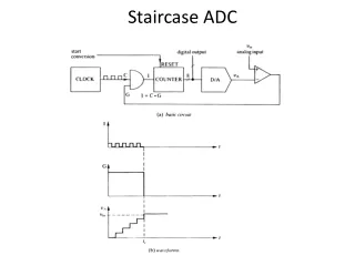
Clock REGISTER COUNTER CONTROL CIRCUIT COUNTER RAMP ADC AND 1) The counter starts to count the clock pulses when the control circuit enables the AND gate. 2)The DAC output is incremented from zero to VFS, by Q-high steps. 3) The counter is stopped as soon as DAC output becomes equal to Vx.
GATE OPEN GATE CLOSED COUNTER RAMP ADC Observations: 1) The maximum number of steps is 2b, when Vx=VFS. Consequently the max sampling frequency is about fSfclock/2b. 2) The ADC errors come from the DAC, in particular from: - the uncertainty on the reference voltage Er. - the uncertainty on the resistance values in the R-2R DACs.
DELTA-SIGMA ADC • Low Cost, High Resolution (to 24-bits) Excellent DNL, • Low Power, but Limited Bandwidth • Key Concepts are Simple, but Math is Complex • Oversampling • Quantization Noise Shaping • Digital Filtering • Decimation • Ideal for Sensor Signal Conditioning • High Resolution • Self, System, and Auto Calibration Modes
ViN(t) t VNA(t) t V1(t) t VC(t) t VU(t) t CLK DELTA-SIGMA ADC: signals t1 t2 t
DELTA-SIGMA ADC Rearranging, solving for y:
HIGH SPEED ADC: interleaving-multiplexing clock VIN fs/M 1 DL S/H A/D 2 DL S/H A/D N 3 S/H DL A/D M S/H A/D
1 2 3 4 5 6 7 8 9 10 1 ns 10 ns HIGH SPEED ADC: interleaving-multiplexing Conversion times


![ADC Architectures[4]](https://cdn2.slideserve.com/4726235/slide1-dt.jpg)