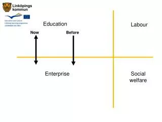
Education:
GOALI: Nanoscale Characterization and Development of Ultra Low-k Dielectric Xerogel Films Richard F. Reidy 1 , M.J. Kim 2 , D.W. Mueller 1 , P.D. Matz 3 , 1 Univ. of North Texas, 2 Univ. of Texas-Dallas, 3 Texas Instruments, DMR 0316916.

Education:
E N D
Presentation Transcript
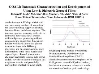
GOALI: Nanoscale Characterization and Development of Ultra Low-k Dielectric Xerogel FilmsRichard F. Reidy1, M.J. Kim2, D.W. Mueller1, P.D. Matz3, 1Univ. of North Texas, 2Univ. of Texas-Dallas, 3Texas Instruments, DMR 0316916 As the features in IC chips shrink with ever increasing numbers of transistors, the interconnecting copper conductors become thinner and closer together. The necessary porous insulating materials or intermetal dielectrics (IMD’s) must withstand plasma processing without compromising copper line dimensions. Recent work have shown that plasma treatments impact the IMD (e.g., roughness and this increased roughness is transferred to the metal barrier and copper layers. Several post-plasma chemical treatments (sample data shown on left) have been shown to mitigate this roughness transfer and potentially prevent loss of effective metal width. Height amplitude profiles from atomic force microscopy (AFM) show that dimethyldimethoxysilane (DMDS) chemical treatments reduce roughness of an H2/N2 plasma treated MSQ film. In short, the chemical treatment reduces the number and severity of surface peaks and valleys.
Education: One undergraduate from the Texas Academy of Mathematics and Science (David Heller), four graduate students (Mingming Du, Casey Smith, Dongkyu Cha), and one postdoctoral fellow (Ekaterina Vinogradova) have contributed to this work. Smith is currently a Nanoscholar Intern at Sematech. Cha is due to graduate in late this Fall. Outreach: On June 16,17,23, Dr. Reidy conducted nanotechnology and semiconductor material demonstrations and hands-on experiments with students of the Texas Governor’s School, a three week program for 152 of the top incoming high school sophomores in Texas. Among the demonstrations were atomic resolution TEM and atomic scale three dimensional reconstructions using the Local Electron Atom Probe. Hands-on efforts included using infrared spectroscopy to identify different materials as part of a forensic analysis. GOALI:Nanoscale Characterization and Development of Ultra Low-k Dielectric Xerogel FilmsR.F. Reidy1, M.J. Kim2, D.W. Mueller1, P.D. Matz3, 1Univ. of North Texas, 2Univ. of Texas-Dallas, 3Texas Instruments, DMR 0316916