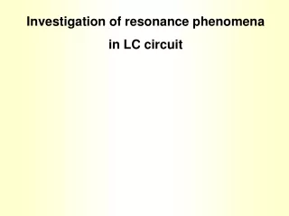
Parallel LC Resonant Circuit
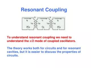
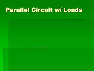
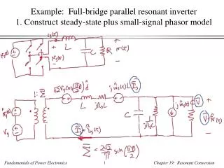
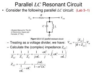
R. V out. V in. C. L. Parallel LC Resonant Circuit. (Lab 3–1). Consider the following parallel LC circuit: Treating as a voltage divider, we have: Calculate the (complex) impedance Z LC :. ( Student Manual for The Art of Electronics , Hayes and Horowitz, 2 nd Ed.).

Parallel LC Resonant Circuit
E N D
Presentation Transcript
R Vout Vin C L Parallel LC Resonant Circuit (Lab 3–1) • Consider the following parallel LC circuit: • Treating as a voltage divider, we have: • Calculate the (complex) impedance ZLC: (Student Manual for The Art of Electronics, Hayes and Horowitz, 2nd Ed.)
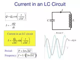
Parallel LC Resonant Circuit • Thus we have: • Note that for (resonant frequency): • Otherwise is small (Remember that w = 2pf)
Parallel LC Resonant Circuit Q = quality factor= f0 / Df3dB = resonance frequency / width at –3 dB points (Remember that at –3 dB point, Vout / Vin = 0.7 and output power is reduced by ½ ) Q is a measure of the sharpness of the peak For a parallelRLCcircuit: • Overall response (Vout / Vinvs. frequency): • This circuit is sometimes called a tank circuit • Most often used to select one desired frequency from a signal containing many different frequencies • Used in radio tuning circuits • Tuning knob is usually a variable capacitor in a parallel LC circuit (The Art of Electronics, Horowitz and Hill, 2nd Ed.)
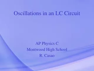
Oscillation in Parallel LC Resonant Circuit (Introductory Electronics, Simpson, 2nd Ed.)
Oscillation in Parallel LC Resonant Circuit • For a pureLCcircuit (no resistance), the current and voltage are exactly sinusoidal, constant in amplitude, and have angular frequency • Can prove with Kirchhoff’s loop rule • Analogous to mass oscillating on a spring with no friction • For an RLC circuit (parallel or series), the current and voltage will oscillate (“ring”) with an exponentially decreasing amplitude • Due to resistance in circuit • Analogous to damped oscillations of a mass on a spring (Lab 3–1) (Introductory Electronics, Simpson, 2nd Ed.)
Series LC Resonant Circuit (HW #1.26) • Consider the following series LC circuit: • Now ZLC = ZC + ZL = jwL – j / wC(L and C in series) • Overall response: (The Art of Electronics, Horowitz and Hill, 2nd Ed.) For seriesRLCcircuit: (The Art of Electronics, Horowitz and Hill, 2nd Ed.)
(Lab 3–1) Fourier Analysis • In Lab 3–1, a parallel LC resonant circuit is used as a Fourier Analyzer • The circuit “picks out” the Fourier components of the input (square) waveform • Fourier analysis: Any function can be written as the sum of sine and cosine functions of different frequencies and amplitudes • We can apply this technique to periodic voltage waveforms: • Where T = minimum time voltage waveform repeats itself and 1 / T = fundamental frequency = f0 • Could instead substitute w = 2p / T
Fourier Analysis • The an and bm constants are determined from: • For a symmetric square wave voltage (assuming V(t) is an odd function): • an = 0 n = 0, 1, 2, 3, …
Fourier Analysis • Thus for a square wave of fundamental frequency w0: • When we apply an input square wave voltage of frequency w0to the parallel LC circuit, we are in essence applying frequencies w0, 3w0, 5w0, etc. simultaneously with relative amplitudes 1, 1/3, 1/5, etc. (respectively) • The LC circuit is a “detector” of its resonance frequency f0, including contributions from the harmonics of the input fundamental frequency • “Mini-resonance” peaks will occur in the output voltage at driving frequencies of f0 / 3, f0 / 5, etc. (Student Manual for The Art of Electronics, Hayes and Horowitz, 2nd Ed.)
Diodes • Diodes are semiconductor devices that are made when p–type and n–type semiconductors are joined together to form a p–n junction • With no external voltage applied, there is some electron flow from the n side to the p side (and similar for holes), but equilibrium is established and there is no net current (Introductory Electronics, Simpson, 2nd Ed.)
Diodes • With a reverse bias external voltage applied, there is only a small net flow of electrons from the p side to the n side, and hence a small positive current from the n to the p side (Introductory Electronics, Simpson, 2nd Ed.)
Diodes • With a forward bias external voltage applied, electrons are “pushed” in the direction they would tend to move anyway, and hence there is a large positive current from the p side to the n side (Introductory Electronics, Simpson, 2nd Ed.)
Diodes (Student Manual for The Art of Electronics, Hayes and Horowitz, 2nd Ed.) • Thus diodes pass current in one direction, but not the other • The diode’s arrow on a circuit diagram points in the direction of current flow When diodes are forward-biased and conduct current, there is an associated voltage drop of about 0.6 V across the diode (for Si diodes) – “diode drop” Current can flow X Current can’t flow
Diodes in Voltage Divider Circuits • Consider diodes as part of the following voltage-divider circuits: (1) • This diode circuit is called a rectifier (specifically, a half-wave rectifier) Vin Vout (Lab 3–2)
Diodes in Voltage Divider Circuits Vin (2) • This circuit is called a diode clamp circuit because the output voltage is “clamped” at about –0.6 V Vout (Lab 3–6)
Diodes in Voltage Divider Circuits (3) • This is another clamp circuit: the output voltage is clamped at about +5.6 V and –0.6 V Vin Vout (Lab 3–6)
Diode Applications • Rectification: conversion of AC to DC voltage • We already saw how this could be done with a half-wave rectifier • A much better way is with a full-wave bridge rectifier: • Two diodes are always in series with the input (so there will always be 2 forward diode drops) • Gap at 0 V occurs because of diodes’ forward voltage drop (Lab 3–3) (The Art of Electronics, Horowitz and Hill, 2nd Ed.)
Diode Applications • Although more efficient than the half-wave rectifier, the bridge rectifier still produces a lot of “ripple” (periodic variations in the output voltage) • The ripple can be reduced by attaching a low-pass filter: • The resistor R is actually unnecessary and is always omitted since the diodes prevent flow of current back out of the capacitors • C is chosen to ensure that RloadC >> 1 / fripple so the time constant for discharge >> time between recharging (Lab 3–4) (The Art of Electronics, Horowitz and Hill, 2nd Ed.)
Diode Applications • We have almost finished building our own DC power supply! • For further power supply design details, see Class 3 Worked Example in the Lab Manual (p. 71–74) (Student Manual for The Art of Electronics, Hayes and Horowitz, 2nd Ed.)
Diode Applications (Lab 3–5) • Signal rectifier • Eliminates an unwanted polarity of a waveform • Example: Remove sharp negative spikes from the output of a differentiator • An RC differentiator is used to generate the spikes, and a diode is used to rectify the spikes: (The Art of Electronics, Horowitz and Hill, 2nd Ed.)
Diode Applications (Lab 3–7) • Voltage limiter • In the circuit below, the output voltage is limited to the range –0.6V Vout +0.6 V • This is just another example of a diode clamp circuit • Useful as an input protection circuit for a high-gain amplifier (otherwise amplifier may “saturate”) (The Art of Electronics, Horowitz and Hill, 2nd Ed.)
Example Problem: Chap. 1 AE 7 Sketch the output for the circuit shown at right. (Solution details will be discussed in class.)