Optimizing SDRAM Performance with Bank Allocation Algorithms for Enhanced Data Access Rates
This paper explores a novel bank allocation algorithm that leverages the unique characteristics of SDRAM to enhance performance in memory and processor systems. Traditional methods such as caching and data prefetching are discussed, but we propose a scheduling method that utilizes SDRAM's multi-bank architecture to improve data access rates. Our experimental results demonstrate significant performance improvements in array assignments across different memory configurations. Future work aims to extend this research to Rambus DRAM and integrate additional scheduling techniques.

Optimizing SDRAM Performance with Bank Allocation Algorithms for Enhanced Data Access Rates
E N D
Presentation Transcript
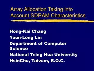
Array Allocation Taking into Account SDRAM Characteristics Hong-Kai Chang Youn-Long Lin Department of Computer Science National Tsing Hua University HsinChu, Taiwan, R.O.C.
Outline • Introduction • Related Work • Motivation • Solving Problem • Proposed Algorithms • Experimental Results • Conclusions and Future Work
Performance gap between memory and processor Systems without cache Application specific Embedded DRAM Optimize DRAM performance by utilize its special characteristics SDRAM’s multi-bank architecture enables new optimizations in scheduling We assign arrays to different SDRAM banks to increase data access rate Introduction
Related Work • Previous research eliminate memory bottleneck by • Using local memory (cache) • Prefetch data as fast as possible • Panda, Dutt, and Nicolau utilizing page mode access to improve scheduling using EDO DRAM • Research about array mapping to physical memories for low power, lower cost, better performance
Motivation • DRAM operations • Row decode • Column decode • Precharge • SDRAM characteristics • Multiple banks • Burst transfer • Synchronous Traditional DRAM 2-bank SDRAM
Address Mapping Table Host Address: [a16:a0] Memory Address: [BA, A7-A0] Page Size for host: Page Size for DRAM: 128words (a6:a0) 256 words (A7:A0) -If we exchange the mapping of a0 and a7...
Motivational Example BA=BankActive =RowDecode R/W=Read/Write =ColumnDecode BP=Precharge
Motivational Example BA=BankActive =RowDecode R/W=Read/Write =ColumnDecode BP=Precharge
Assumptions • Harvard architecture : Separated program/data memory • Paging policy of the DRAM controller • Does not perform precharge after read/write • If next access reference to different page, perform precharge, followed by bank active, before read/write • As many pages can be opened at once as the number of banks • Resource constraints
Problem Definition • Input a data flow graph, the resource constraints, and the memory configuration • Perform our bank allocation algorithm • Schedule the operations with a static list scheduling algorithm considering SDRAM timing constraints • Output a schedule of operations, a bank allocation table, and the total cycle counts
Bank Allocation Algorithm • Calculate Node distances • Calculate Array distances • Give arrays with the shorter distances higher priority • Allocate arrays to different banks if possible
Example: SOR main() { float a[N][N], b[N][N], C[N][N], d[N][N], e[N][N], f[N][N]; float omega, resid, u[N][N]; int j,l; for (j=2; j<N; j++) for (l=1;l<N;l+=2) { resid = a[j][l]*u[j+1][l]+ b[j][l]*u[j-1][l]+ c[j][l]*u[j][l+1]+ d[j][l]*u[j][l-1]+ e[j][l]*u[j][l] – f[j][l]; u[j][l] -= omega*resid/e[j][l]; } }
Node Distance • Distances between current node and the nearest node that access array a, b, c,…. Shown in { } • Ex. {1,-,-,-,-,-,-,1,-} means the distances to the node that access array a[j] and u[j-1] are both 1. • ‘-’ means the distance is still unknown • When propagate downstream, the distance increases.
Array Distance • The distance between nodes that access arrays • Calculate from node distance of corresponding arrays • Get the minimum value • Ex. AD(a[j], u[j-1])=min(2,4)=2
Example: SOR Bank allocation: Bank 0: c,d,e,f Bank 1: a,b,u
Experimental Characteristics • We divided our benchmarks into two groups • First group benchmarks access multiple 1-D arrays • Apply our algorithm to arrays • Second group benchmarks access single 2-D arrays • Apply our algorithm to array rows • Memory configurations • Multi-bank configuration: 2 banks/ 4banks • Multi-chip configuration: 2 chips/ 4chips • Multi-chip vs mulit-bank: relieves bus contention • Utilizing page mode access or not
Experimental Results • From the average results, we can see that • Scheduling using SDRAM with our bank allocation algorithm do improve the performance • Utilizing page mode access relieves the traffic of address bus, thus the use of multiple chips does not make obvious improvement
Conclusions • We presented a bank allocation algorithm incorporated in our scheduler to take advantages of SDRAM • The scheduling results have a great improvement from the coarse one and beat Panda’s work in some cases • Our work is based on a common paging policy • Several different memory configurations are exploited • Scheduling results are verified and meet Intel’s PC SDRAM’s spec
Future Works • Extending our research to Rambus DRAM • Grouping arrays to incorporating burst transfer • Integration with other scheduling /allocation techniques