Download
1 / 34
340 likes | 481 Vues
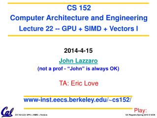
www-inst.eecs.berkeley.edu/~cs152/. CS 152 Computer Architecture and Engineering. Lecture 22 -- GPU + SIMD + Vectors I. 2014-4-15 John Lazzaro (not a prof - “John” is always OK). TA: Eric Love. Play:. Today: Architecture for data parallelism. The Landscape: Three chips that deliver

E N D
www-inst.eecs.berkeley.edu/~cs152/ CS 152 Computer Architecture and Engineering Lecture 22 -- GPU + SIMD + Vectors I 2014-4-15 John Lazzaro (not a prof - “John” is always OK) TA: Eric Love Play:
Today: Architecture for data parallelism The Landscape: Three chips that deliver TeraOps/s in 2014, and how they differ. E5-2600v2: Stretching the Xeon server approach for compute-intensive apps. Short Break GK110: nVidia’s flagship Kepler GPU, customized for compute applications.
4 single- precision multiply-adds issue in lockstep (SIMD) per cycle. Sony PS3 Cell Processor SPE Floating-Point 6 cycle latency (in blue) Single-Instruction Multiple-Data 6 gamer SPEs, 3.2 GHz clock, --> 150 GigaOps/s
Sony PS3 Cell Processor SPE Floating-Point Single-Instruction Multiple-Data In the 1970s a big part of a computer architecture class would be learning how to build units like this. Top-down (f.p. format) && Bottom-up (logic design)
Sony PS3 Cell Processor SPE Floating-Point Today, the formats are standards (IEEE f.p.) and the bottom-up is now “EE.” The PS3 ceded ground to Xbox not because it was underpowered, but because it was hardtoprogram. Architects focus on how to organize floating point units into programmable machines for application domains.
Intel E5-2600v2 12-core Xeon Ivy Bridge 0.52 TeraOps/s Haswell: 1.04 TeraOps/s 12 cores @ 2.7 GHz Each core can issue 16 single-precision operations per cycle. $2,600 per chip
Kepler GK 110 nVidia GPU 5.12 TeraOps/s 2880 MACs @ 889 MHz single-precision multiply-adds $999 GTX Titan Black with 6GB GDDR5 (and 1 GPU)
XC7VX980T (die photo of a related part) Xilinx Virtex 7 with the most DSP blocks. 5.14 TeraOps/s 3600 MACs @ 714MHz Comparable to single-precision floating-point. $16,824 per chip Typical application: Medical imaging scanners, for first stage of processing after the A/D converters.
Intel E5-2600v2 12 cores @ 2.7 GHz 12 cores @ 2.7 GHz Each core can issue 16 single-precision ops/cycle. Haswell cores issue 32/cycle. How?
Advanced Vector Extension (AVX) unit Smaller than L3 cache, but larger than L2 cache. Relative area has increased in Haswell Die closeup of one Sandy Bridge core
Programmers Model 8 128-bit registers Each register holds 4 IEEE single-precision floats The programmers model has many variants, which we will introduce in the slides that follow AVX IA-32 Nehalem
XMM2 XMM3 op = * XMM4 Multiply two 4-element vectors of single-precision floats, element by element. New issue every cycle. 5 cycle latency (Haswell). Example AVX Opcode VMULPS XMM4 XMM2 XMM3 Aside from its use of a special register set, VMULPS execute like normal IA-32 instructions.
Sandy Bridge, Haswell Sandy Bridge extends register set to 256 bits: vectors are twice the size. IA-64 AVX/AVX2 has 16 registers (IA-32: 8) Haswell adds 3-operand instructions a*b + c Fused multiply-add (FMA) 2 EX units with FMA --> 2X increase in ops/cycle
OoO Issue Haswell sustains 4 micro-op issues per cycle. Haswell has two copies of the FMA engine, on separate ports. One possibility: 2 for AVX, and 2 for Loads, Stores and book-keeping. Haswell (2013)
AVX: Not just single-precision floating-point AVX instruction variants interpret 128-bit registers as 4 floats, 2 doubles, 16 8-bit integers, etc ... 256-bit version -> double-precision vectors of length 4
Exception Model Floating-point exceptions: Always a contentious issue in ISA design ... MXCSR: AVX condition codes register
Exception Handling Or, configure AVX for show must go on semantics: on error, results are set to +Inf, -Inf, NaN, ... Use MXCSR to configure AVX to halt program for divide by zero, etc ...
Data moves AVX register file reads pass through a permute and shuffle networks in both “X” and “Y” dimensions. Many AVX instructions rely on this feature ...
Or, part of a math opcode. Pure data move opcode.
Arbitrary data alignment Shuffling two vectors. Permutes over 2 sets of 4 fields of one vector.
Memory System Gather: Reading non-unit-stride memory locations into arbitrary positions in an AVX register, while minimizing redundant reads. Values in memory. Specified indices. Final result.
Positive observations ... If you’re planning on experimenting with GPUs, you need a Xeon server anyway ...aside from $$$, why not buy a high-core-count variant? Applications that do “a lot of everything” -- integer, random-access loads/stores, string ops -- gain access to a significant fraction of a TeraOp/s of floating point, with no context switching. Best for applications that are a good fit for Xeon’s memory system: Large on-chip caches, up-to-a-TeraByte of DRAM, but only moderatebandwidth requirements to DRAM.
Negative observations ... AVX is difficult for compilers. Ideally, someone has written a library of hand-crafted AVX assembly code that does exactly what you want. AVX changes each generation, in a backward compatible way, to add the latest features. Two FMA units per core (50% of issue width) is probably the limit. So, scaling vectorsize or scaling corecount are the only upgrade paths. 0.52 TeraOp/s (Ivy Bridge) << 5.12 TeraOp/s (GK110) And $2700 (chip only) >> $999 (Titan Black card). 59.6 GB/s << 336 GB/s (memory bandwidth)
Break Play:
Kepler GK 110 nVidia GPU The granularity of SMX cores (15 per die) matches the Xeon core count (12 per die)
SMX core (28 nm) Sandy Bridge core (32 nm)
889 MHz GK 110 SMX core vs 2.7 GHz Haswell core 4X single-precision, 1.33X double-precision 1024-bit SIMD vectors: 4X more than Haswell 32 single-precision floats or 16 double-precision floats single prec. double prec. Execution units vs. Haswell 3X (single-precision), 1X (double-precision) Clock speed vs Ivy Bridge Xeon: 3X slower
Thread scheduler Organization: Multi-threaded like Niagara 2048 registers in total. Several programmer models available. Largest model has 256 registers per thread, supporting 8 active threads.
Thread scheduler Organization: Multi-threaded, In-order Each cycle, 3 threads can issue 2 in-order instructions. The SIMD math units live here
Bandwidth to DRAM is 5.6X Xeon Ivy Bridge But, DRAM limited to 6GB, and all caches are small compared to Xeon
Kepler GK 110 nVidia GPU 5.12 TeraOps/s 2880 MACs @ 889 MHz single-precision multiply-adds $999 GTX Titan Black with 6GB GDDR5 (and 1 GPU)
On Thursday To be continued ... Have fun in section !