Photodiodes
300 likes | 711 Vues
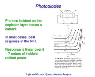
Chapter 9. Optoelectronic Diodes. Photodiodes. Reverse current due to carriers swept by the E -field. Electron-hole pair generation due to light. Chapter 9. Optoelectronic Diodes. I –V Characteristics and Spectral Response. Open circuit voltage v oc.

Photodiodes
E N D
Presentation Transcript
Chapter 9 Optoelectronic Diodes Photodiodes Reverse current due to carriersswept by the E-field Electron-hole pair generation due to light
Chapter 9 Optoelectronic Diodes I–V Characteristics and Spectral Response Open circuit voltage voc Upper limit ~ highest wavelength ~ lowest frequency ~ lowest energy Short circuit current isc
W ≈Wi-region most carriers are generated in the depletion faster response time (~10 GHz operation) Chapter 9 Optoelectronic Diodes p-i-n Photodiodes p-i-n : positive–intrinsic– negative Reverse biased • current arises mostly in the totally depleted i-region, not in quasineutral region as in pn diode • generated carriers do not need to diffuse into the depletion region before they are swept by the E-field • enhanced frequency response
Chapter 9 Optoelectronic Diodes Light Emitting Diodes (LEDs) Increasing EG Forward bias • LEDs are typically made of compound semiconductors (direct semiconductors with band-to-band recombination) • It releases energy by dissipating light / emitting photon
Chapter 10 BJT Fundamentals Bipolar Junction Transistors (BJTs) • Over the past decades, the higher layout density and low-power advantage of CMOS (Complementary Metal–Oxide–Semiconductor) has eroded away the BJT’s dominance in integrated-circuit products. • Higher circuit density better system performance • BJTs are still preferred in some digital-circuit and analog-circuit applications because of their high speed and superior gain • Faster circuit speed (+) • Larger power dissipation (–) • Transistor: current flowing between two terminals is controlled by a third terminal
Chapter 10 BJT Fundamentals Introduction • There are two types of BJT: pnp and npn. • The convention used in the textbook does not follow IEEE convention, where currents flowing into a terminal is defined as positive. • We will follow the normal convention: . . . . . .
Chapter 10 BJT Fundamentals Circuit Configurations Common-Emitter I–V Characteristics Most popular configuration Active Mode Saturation Mode IC < bIB In active mode, bdc is the common emitter dc current gain
Chapter 10 BJT Fundamentals Modes of Operation • Common-Emitter Output Characteristics
Chapter 10 BJT Fundamentals BJT Electrostatics • Under equilibrium and normal operating conditions, the BJT may be viewed electrostatically as two independent pn junctions. W : quasineutral base width
Chapter 10 BJT Fundamentals BJT Electrostatics • Electrostatic potential, V(x) • Electric field, E(x) • Charge density, ρ(x)
Chapter 10 BJT Fundamentals BJT Design • Important features of a good transistor: • Injected minority carriers do not recombine in the neutral base region short base, W << Lp for pnp transistor • Emitter current is comprised almost entirely of carriers injected into the base rather than carriers injected into the emitter the emitter must be doped heavier than the base pnp BJT, active mode
Chapter 10 BJT Fundamentals 3 2 4 1 Base Current (Active Bias) • The base current consists of majority carriers (electrons) supplied for: • Recombination of injected minority carriers in the base • Injection of carriers into the emitter • Reverse saturation current in collector junction • Recombination in the base-emitter depletion region EMITTER COLLECTOR BASE n-type p-type p-type
Chapter 10 BJT Fundamentals 2 2 1 1 5 BJT Performance Parameters (pnp) IEn ICn Negligible compared to holes injected from emitter ICp IEp • Emitter Efficiency • Base Transport Factor • Decrease relative to and to increase efficiency • Decrease relative to to increase transport factor Common base dc current gain:
Chapter 10 BJT Fundamentals 3 2 Collector Current (Active Bias) • The collector current is comprised of: • Holes injected from emitter, which do not recombine in the base • Reverse saturation current of collector junction ICB0 :collector current when IE = 0 Common emitter dc current gain:
Chapter 11 BJT Static Characteristics Notation (pnp BJT) Minority carrier constants
Chapter 11 BJT Static Characteristics Emitter Region • Diffusion equation: • Boundary conditions:
Chapter 11 BJT Static Characteristics Base Region • Diffusion equation: • Boundary conditions:
Chapter 11 BJT Static Characteristics Collector Region • Diffusion equation: • Boundary conditions:
Chapter 11 BJT Static Characteristics Ideal Transistor Analysis • Solve the minority-carrier diffusion equation in each quasi-neutral region to obtain excess minority-carrier profiles • Each region has different set of boundary conditions • Evaluate minority-carrier diffusion currents at edges of depletion regions • Add hole and electron components together terminal currents is obtained IC IE IB
Chapter 11 BJT Static Characteristics Emitter Region Solution • Diffusion equation: • General solution: • Boundary conditions: • Solution
Chapter 11 BJT Static Characteristics Collector Region Solution • Diffusion equation: • General solution: • Boundary conditions: • Solution
Chapter 11 BJT Static Characteristics Base Region Solution • Diffusion equation: • General solution: • Boundary conditions: • Solution
Chapter 11 BJT Static Characteristics Base Region Solution • Since • We can write as
Chapter 11 BJT Static Characteristics Base Region Solution • Since
Chapter 11 BJT Static Characteristics Terminal Currents • Since • Then
Chapter 11 BJT Static Characteristics Simplified Relationships • To achieve high current gain, a typical BJT will be constructed so that W << LB. • Using the limit value Due to VEB • We will have Due to VCB
Chapter 11 BJT Static Characteristics Performance Parameters • For specific condition of • “Active Mode”: emitter junction is forward biased and collector junction is reverse biased • W << LB, nE0/pB0 = NB/NE
Chapter 6 pn Junction Diodes: I-V Characteristics Homework 7 • 1. (10.17) • Consider a silicon pnp bipolar transistor at T = 300 K with uniform dopings of NE = 5×1018 cm–3, NB = 1017 cm–3, and NC = 5×1015 cm–3 . Let DB = 10 cm2/s, xB = 0.7 μm, and assume xB << LB. The transistor is operating in saturation with JP = 165 A/cm2 and VEB = 0.75 V. Determine: • (a) VCB, (b) VEC(sat), (c) the number/cm2 of excess minority carrier holes in the base, and (d) the number/cm2 of excess minority carrier electrons in the long collector, take LC = 35 μm. • 2. (10.14) • Problem 10.4, Pierret’s “Semiconductor Device Fundamentals”. • Deadline: 07.04.2011, at 07:30 am.