PVD (Physical Vapor Deposition ) Technology
2.81k likes | 5.63k Vues
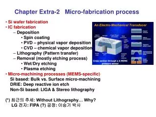
PVD (Physical Vapor Deposition ) Technology . tsmc FAB 14 吳佳俊. Outline. What is Plasma Convention PVD Process (DC plasma) DC Plasma PVD bottle neck What is RF ( Radio frequency ) PVD Chamber H/W Evolution Metal line process overview tsmc introduction EE responsibility Q & A.

PVD (Physical Vapor Deposition ) Technology
E N D
Presentation Transcript
PVD (Physical Vapor Deposition )Technology tsmc FAB 14 吳佳俊
Outline • What is Plasma • Convention PVD Process (DC plasma) • DC Plasma PVD bottle neck • What is RF ( Radio frequency ) • PVD Chamber H/W Evolution • Metal line process overview • tsmc introduction • EE responsibility • Q & A
What is Plasma ? • 電 Electrical Particles • 漿 Collective motion • It contains highly reactive gas species • It emits light glow (O2->whitish-blue, N2->pink) • It is driven by electric energy electric field
Plasma Components • Created by current through a gas • Gas is partially ionized • Quasi-neutral plasma • Nearly equal numbers of positive ( ) and negative ( )
Basic Plasma Concept • Ionization • Initially, very few electrons are present in neutral gas • The electrons are accelerated by energy input • Newly produced electrons accelerate and ionize more neutrals • Ionized avalanche happened • Equi-potential cloud plasma is formed
Basic Plasma Concept • Excitation-Relaxation • Light is emitted
Basic Plasma Concept • Dissociation • When an electron collides with a molecule with enough energy • Break its bonding energy into apart • Much less energy than ionization • Much higher dissociation rate than ionization
DC Plasma • Initiation of The Plasma • Plasma is formed when an avalanche of ionization occurs • This results in a sea of positive and negative charged particles • The gas into plasmas transition involves going from insulating medium to conductive medium
PVD Dry-ETCH HDP-CVD Basic Plasma Concept • Steady plasma source • Energetic electron (Plasma type) • Appropriate collision (Recipe) • Plasma sustain (Geometry design)
PVD(Physical Vapor Deposition) Process (DC plasma Deposition)
Sputtering • Momentum transfer will dislodge surface atom off • About 70% energy converts to heat • About 25% energy generates secondary electrons • Secondary electrons ionize Ar
DC Magnets Sputtering • Film Uniformity • High target utilization • Full face erosion • Plasma ignition & sustaining • Step coverage
Convention PVD (DC Plasma) • Target (Metal source) • Plasma • Gas • Pump • Pedestal
-V Pedestal Convention PVD Process • Ion generated & toward a target • Atoms sputter from target • Sputtered atoms traverse to substrate • Condense • Nucleated • Form a film
Film Growth Overview • Formation of isolated nuclei • Island formation • Formation continuous film grain boundaries • Grain growth
W h SiO2 DC Plasma PVD Bottle Neck • Aspect Ratio (h/w) • Step Coverage
Collimator PVD • Lower deposition rate • Potential Particle issue • Shorter PM cycle
Long throw PVD • Lower deposition rate • Worse film uniformity • Shorter PM cycle L
PVD(Physical Vapor Deposition) Process (RF plasma Deposition)
RF microwave audio 20 kHz 300 MHz What is RF ? • AC frequencies
13.56MHz Radio Frequency Radio frequency
Why need to use AC Plasma ? • Step Coverage Ration
DC Biasing of RF • RF power couples through the wafer like a capacitor • On-average, the wafer is biased negative (attracts ions)
RF Power • Forward Power • Power from RF generator • Reflected Power • Power return to RF generator • Load Power • Power consumed by load Direction Coupler
Impedance (Z) • Made up of two parts • Resistance • Reactance (Capacitive & Inductive) • Most RF generator are designed to operate into a 50 load • Plasma impedance ZL dependent on Power • Gas pressure and chemistry • Power level and frequency • Chamber materials and geometry’s
Maximum Power Theorem • Maximum power when ZS = ZL • RF generator ZS = (50 j0) • ZS ZL Reflected power increased • RF tuner is required to transform ZS = ZL
RF Matching Network • Manual match • Auto match • Air capacitor (for low power / fast response) • Vacuum capacitor (for high power / low response) • Fixed match • The most fast response / acceptable reflected power at certain VSWR • Switching match (fast response)
IMP (Ion Metal Plasma) Chamber • DC RF source generate Medium density Plasma • Add coil DC • Coil sputtering, blocking capacitor • Increase pedestal bias potential
SIP Technology • Self ionized Plasma • Sputter discharge in which the dominate ionized species is from the target • Higher ionization rate and enough self-sputter yield to sustain plasma without Ar gas • Plasma Characteristics • High power • Low pressure
SIP Process • Large wafer to target spacing • Leads to “long-throw” directional trajectories for neutral • Unbalance Magnet • Control ion trajectories • Cooled, biased substrate
Ch D (PC II) FI PVD 4 (Cu) Ta Ch F (Degas) PVD 3 (TaN) TaN SWLL B LP 2 SWLL A PVD 2 (TaN) Ch E (Degas) PVD 1 (Cu) Ch C (PC II) LP 1 AMAT EnCoRe Barrier/Cu Seed