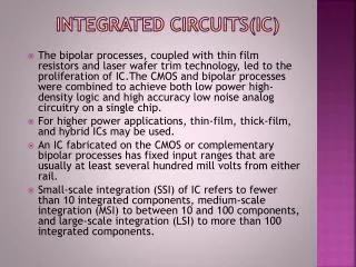
INTEGRATED CIRCUITS
INTEGRATED CIRCUITS. Dr. Esam Yosry. Lec . #5. Introduction Epitaxy Deposition Chemical Vapor Deposition (CVD) Physical Vapor Deposition (PVD ) Molecular Beam Epitaxy (MBE ) Metal Deposition Manufacturing Methods CVD and PVD. Epitaxial Growth.


INTEGRATED CIRCUITS
E N D
Presentation Transcript
INTEGRATED CIRCUITS Dr. EsamYosry Lec. #5
Introduction • Epitaxy • Deposition • Chemical Vapor Deposition (CVD) • Physical Vapor Deposition (PVD) • Molecular Beam Epitaxy (MBE) • Metal Deposition • Manufacturing Methods • CVD and PVD Epitaxial Growth
Introduction(Processes) • Oxidation • Diffusion • Ion Implantation • Deposition • Etching • Lithography • Deposition • Removal • Patterning • Modification of electrical properties
Epitaxy • Epitaxy is the process of growing a crystalline layer of a material on top of a crystalline substrate . • Epitaxial means arranged upon (epi). • The epi silicon layer is usually of different doping. • Single crystal of Si over crystalline Si substrate • Epi layer can be doped independent of substrate
Epitaxy • Necessary if buried layers are needed • Needed to form isolation islands in bipolar • Grown by CVD or MBE • An epitaxial layer can be doped during deposition by adding impurities to the source gas. • The concentration of impurity in the gas determines its concentration in the deposited film
Selective Epitaxial Growth (SEG) • Nucleation rate: Si > Si3N4 > SiO2 • Used for deviceisolation
Deposition • Depositing a material onto a substrate or onto previously deposited layers. • Thin-film deposition: layer thickness within a few tens of nanometres. • Molecular Beam Epitaxy (MBE): allows a single layer of atoms to be deposited at a time. • (layers of insulators, semiconductors, conductors) • Deposition techniques: Chemicalor Physical
Chemical Deposition • Chemical change at a solid surface, leaving a solid layer. • Chemical Vapor Deposition (CVD): uses a gas-phase, often a halide or hydride of the element to be deposited.
Physical Deposition • Uses mechanical, electromechanical or thermodynamic means to produce a thin film of solid. • Molecular Beam Epitaxy(MBE) :slow streams of an element can be directed at the substrate, so that material deposits one atomic layer at a time.
Chemical Vapor Deposition (CVD) • CVD is a chemical process used to produce high-purity, high-performance solid materials • Needs a CVD reactor at around 1000o C • Typical Si sources: *silicon tetrachloride SiCl4 (STC) *silane SiH4
Chemical Vapor Deposition (CVD) • Process: 1. Wafers are on a heated substrate holder. 2. Process gases are flowed into the system. 3. Chemical reaction occurs at the wafer surface. Hot wafer surface accelerates the reaction. 4. Solid material which deposits on the wafer. • CVD used to deposit materials in: monocrystalline, polycrystalline, amorphous, and epitaxial (single crystal)
Chemical Vapor Deposition (CVD) • Commercially materials prepared by CVD Polysilicon: SiH4 Si + 2H2 (low T) (single crystal) Si Dioxide: SiH4+O2 SiO2+2H2 (amorphous) Si Nitride: SiH4+4NH3 Si3N4+12H2 Silicon nitride is often used as an insulator and chemical barrier in manufacturing ICs
Chemical Vapor Deposition (CVD) Types Classified by operating pressure: • Atmospheric pressure CVD (APCVD). • Low-pressure CVD (LPCVD) – CVD at sub-atmospheric pressure. Reduced pressures tend to reduce unwanted gas-phase reactions and improve film uniformity across the wafer. • Ultrahigh vacuum CVD (UHVCVD) – CVD at very low pressure.
Physical Vapor Deposition (PVD) • Describes a variety of vacuum deposition methods used to deposit thin films by a vaporized form of the desired film material onto wafers. • These methods are purely physical processes such as high-temperature vacuum evaporation with subsequent condensation, or plasma sputter bombardmentrather than a chemical reaction at the surface as in chemical vapor deposition.
Bell Jar Physical Vapor Deposition (PVD) • Mostly line-of-sight since low pressure. • Deposition rate is determined by emitted flux and by geometry of target.
Molecular Beam Epitaxy (MBE) • Thermal evaporation is used instead of CVD • Evaporation in Ultra High Vacuum (10-10Torr) • “molecular beam” since the UHV pressure causes a pure beam of molecules incident on the substrate • Multiple material sources are used to make doping • Low temperature process • Precise doping control
Molecular Beam Epitaxy (MBE) • Suitable for heteroepitaxy (layers of compounds) • Doping during deposition or after • Expensive equipment (compared to reactors) • Atomically smooth interface • Can use low deposition rate
CVD and PVD • Isotropic arrival angle • High pressure • Chemical reaction • Vertical arrival angle • Low pressure • No chemical reaction
Metal Deposition evaporation • Metal evaporation can’t ensure metal continuity for large contact window aspect ratio (shadowing effect and step coverage problems) • CVD can fill a contact window more efficiently (this is called a plug process) CVD plug Incomplete fill
Aluminum Deposition • To obtain a thin-uniform coating of aluminum, one must spray or evaporate it from a liquid form. • Aluminum melts at 600°C but will not evaporate at atmospheric pressure (Low pressure is required). • Evaporation must be in a non-oxidizing ambient to prevent formation of Al2O3 and keep slow. • Deposition could be done by sputtering, chemical vapor deposition, or evaporation. We choose Evaporation because it is simple.
Thanks Many thanks to Prof. Hany Fikry and Prof WaelFikry for their useful materials that help me to prepare this presentation.