Integrated Circuits
Integrated Circuits. How are Integrated Circuits Made?.


Integrated Circuits
E N D
Presentation Transcript
How are Integrated Circuits Made? An integrated circuit or IC is basically the assembly of electronic components fabricated on a semiconductor material as a unit. There are different techniques used to design and construct integrated circuits. In today's world, integrated circuits are used in almost all electronic equipment.
Integrated Circuits • An Integrated circuit (IC, microchip, or chip) is an electronic circuit made up of small semiconductor devices and other electronic components that are manufactured on a semiconductor material.
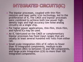
Integrated Circuits// • The integration of a large number of transistors into a single chip was a great achievement. It was only made possible after conducting a great number of experiments, and then it was discovered that semiconductor devices could perform the functions of vacuum tubes. The first integrated chip was designed by Jack S Kilby at Texas Instruments in 1958.
Advantages of ICs • The discovery of integrated circuits was a huge breakthrough in the field of electronics due to the fact that ICs were a lot more reliable, capable, and cheaper than discrete circuits.
// Advantages of ICs • Also the space occupied by the electronic components is minimized as all the components are printed as a unit and much less material is required. • Power consumption is another advantage of ICs because the components are very small in size and are working as a unit.
Designing • There are certain circuit design and logic techniques that are used to design an integrated circuit. There are two categories of IC design which are: • . • Digital design • Analog Design
Designing • Microprocessors, memories (RAM, ROM) . are designed by Digital IC design method. Digital designing ensures that the circuits are correct and the circuit density is at maximum. The overall efficiency of the circuit is very high.
Designing • On the other hand, Analog design method is used to design oscillators, filters, line regulators, operational amplifiers and phase locked loops. • Analog designing is used where gain, power dissipation and resistance are required to be perfect. • Automated design tools are used to design such circuits as the demand is increasing alarmingly and designs needs to be made very rapidly.
Design Steps • There are some steps in the design process which need to be followed very carefully and efficiently. • These steps are as follows: • 1- Size estimation and feasibility report • 2- Circuit Design • 3- Circuit Simulation • 4- Review of the Design
Design Steps • 6- Design Layout • 7- Timing Analysis • 8- Automatic test pattern generation • 9- Manufacturing design • 10- Mask data preparation • 11- Fabrication of Wafer • 12- Die test • 13- Packaging
Design Steps • 14- Device Characterization • 15- Generating the Data Sheet • 16- Final Production • 17- Reliability Analysis • 18- Failure Analysis
Electronic System LevelDesign • The digital design comprises "ESL Design." All the user specifications of the functions are created in it. It is created in programming languages such as C++, Verilog, Matlab, etc. • Then comes "RTL Design."
Register Transfer Level • The user specifications in the ESL design are then converted into "Register Transfer Level" description. RTL defines the interconnections to the outputs and inputs. The last is the "Physical Design." In this step, the final chip design is created by using the RTL and logic gates.
Analog Design • In Analog Design, circuit simulation tools are used to design the ICs with high efficiency and make complex calculations. The first circuit simulator that was used for this purpose was called "SPICE."
// Analog Design • If there are any mistakes in the design cycle, the circuit simulation tools find them so that they can be fixed before the fabrication process. Also other factors such as temperature and doping concentration can be monitored continuously to determine if the design is ready to be fabricated.
Construction and Manufacturing • There are two main steps in the manufacturing process : • Fabrication • Packaging
1. Fabrication • The process of creating integrated circuits is called Fabrication. It is a sequence of chemical and photographic steps in which the circuits are constructed on a semiconductor material known as "wafer". The steps are described below:
Lithography • In this step, a layer of photo-resisting liquid is applied on the surface of semiconductor or wafer. It is then backed and hardened. • Etching • In etching process, unwanted material is removed from the wafer. Then the pattern of the photo-resist is transferred to the wafer.
Thermal and electrical conduction properties of semiconductors are changed through etching.
Deposition • In this step, films of different materials are applied on the wafer.It is done by either "Physical Vapor Deposition" or "Chemical Vapor Deposition". • Oxidation • In the oxidation process, the silicon layers on the top are converted to silicon dioxide by oxygen or water molecules.
Diffusion • Diffusion can be defined as the random walk of an ensemble of particles from regions of high concentration to regions of lower concentration. In integrated circuit fabrication, diffusion is used to introduce dopants in controlled amounts into the semiconductor substrate. In particular, diffusion is used to: • form the base and emitter in bipolar transitors • form integrated resistors
Packaging • Packaging is also called "encapsulation" or "assembly". It is the final stage of IC manufacturing. In the beginning, ICs were packaged in ceramic flat packs. This technique was used for some years then the "Dual in-line package"(DIP) was introduced.
Packaging • With the passage of time other techniques were introduced such as "Pin Grid Array" and "Surface mount." Intel and AMD have moved to "land Grid array" packages.
Packaging • The packaging process also has some steps that have to be followed which are given below: • Die attaching • IC Bonding • Flip Chip • Quilt Packaging • Film Attaching • IC encapsulation
Packaging • Integrated circuits are mostly packaged in opaque plastic or ceramic insulation. There are metal pins in the packaging which are used to connect to the outside world.