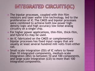
INTEGRATED CIRCUITS
INTEGRATED CIRCUITS. Dr. Esam Yosry. Lec . #6. Lithography. Introduction Lithography Photolithography Photoresist Process Types of Photoresist Photomask Clean Rooms. Introduction ( Chip Fabrication Cycle). Introduction ( Processes). Oxidation Diffusion Ion Implantation Deposition


INTEGRATED CIRCUITS
E N D
Presentation Transcript
INTEGRATED CIRCUITS Dr. EsamYosry Lec. #6
Lithography • Introduction • Lithography • Photolithography • Photoresist Process • Types of Photoresist • Photomask • Clean Rooms
Introduction(Processes) • Oxidation • Diffusion • Ion Implantation • Deposition • Etching • Lithography • Deposition • Removal • Patterning • Modification of electrical properties
Lithography • Lithography is the process of transferring patterns drawn on a mask to a thin layer of radiation sensitive material (resist) covering the surface of the material to be etched (oxide or metal). • The main equipment is optical ultraviolet unit (UV wavelength 200 to 400 nm). • In this case the mask is called photomask (PM), the resist is called photoresist (PR) and the process is called photolithography.
Lithography • Patterning process consists of mask design, mask fabrication and wafer printing.
Lithography • In case of X-ray (wavelength 0.2 to 5 nm) the resist is called X-ray resist and the process is called X-ray lithography. • In electron-beam (EB) lithography (wavelength ≈ 0.1 nm) using EB resist. • The shorter the radiation wavelength the smaller the feature size that can be produced. • Since the EB radiates very small spots, no mask is needed and direct exposure of the EB resist is carried out (serial exposure of the resist or direct writing on the resist).
Lithography • When masks are used (photo- and X-ray- lithography), we irradiate the whole resist surface using parallel exposure. • EB lithography is used when the product volume is small because masks are very expensive to fabricate. • Masks are themselves fabricated by EB lithography for shaping chromium metallic layer deposited on quartz transparent supports. • Masks are only used to reproduce very large number of wafers exceeding 10000.
As processing equipment and technologies become more advanced, transistor size shrinks • In the 70’s, 8 • Now, 0.02 • This is due to advancement in lithography • . • Each layer of dopant or material has its own layout (15 – 20 mask). Lithography
Photolithography Photolithography is the heart of integrated circuit processing. It is the method used to transfer the individual circuit design knowledge onto the silicon wafer. Probably one half of the wafer fabrication costs go into obtaining proper photolithography. The basic elements consist of: • An Align and Expose Tool • Masks containing design information • Photo-sensitive Resist
Basics of Photolithography Silicon Wafer with Silicon Dioxide SiO2 To be etched Silicon Wafer
Basics of Photolithography Apply photo resist Photoresist SiO2 Silicon Wafer
Basics of Photolithography Apply photomask Photomask SiO2 Silicon Wafer
Basics of Photolithography Apply Ultraviolet Light Photomask SiO2 Silicon Wafer Decreasing feature size require the use of shorter λ
Basics of Photolithography Develop photoresist SiO2 Silicon Wafer
Basics of Photolithography Etch Silicon Dioxide SiO2 Silicon Wafer
Basics of Photolithography Strip Photoresist SiO2 Silicon Wafer
Photoresist Process This flow chart shows the typical process used for VLSI Lithography.
Photoresist Process 1. Substrate Cleaning and Preparation • The surface is as clean as possible immediately after a high temp operation. • Acid cleaning may be necessary if wafers sit for a long time.
Photoresist Process 2. Wafer Coating The goal of coating is to apply a uniform, defect free film of photoresist over The entire wafer. Spin Coating is used for VLSI • accelerate the wafer - fast • spin at constant speed to get uniform thickness Before spin After spin PR Wafer PR Chuck
Photoresist Process 3. Pre-Bake (Soft-Bake) The Soft-Baked is used to: • Drive off solvent from resist. (reduced to ~5%) • Improve adhesion and anneal stresses in resist Typical process Temp is 90-100°C Ovens • Convection oven - Very stable over time. ~ 30 min • IR oven - Most popular. 3-4 min. • Hot plate - very effective for single wafers.
Photoresist Process 4. Expose Photomask To produce the desired photochemical effects in the shortest time possible. Time is important because: • Wafers are individually processed • Align machines are expensive However, short times usually mean lower resolution. Exposure to UV light chemically changes the resist SiO2 Silicon Wafer
Photoresist Process 5. Develop SiO2 Silicon Wafer Development removes the unwanted photoresist. • Positive Resist - Area exposed is removed • Negative Resist - Area not exposed is removed
Photoresist Process 6. Post-Bake 100-120°C 30 minutes • Hardens Resist Prior to Etch • Temperature is critical • Too high a Temp (>120°C) causes resist to flow • Extra high Temp (>180°C) causes resist to lift.
Photoresist Process 7. Inspection • The object of this inspection is to verify the photoresist is acceptable prior to etch. • A complete rework can now be performed if the photoresist is not acceptable.
Photoresist Process 8. Etch SiO2 • Dry Plasma Etch is commonly used in commercial manufacturing lines. • We use Wet Etch with acids because of the cost and flexibility of the process. Silicon Wafer
Photoresist Process 9. Strip SiO2 Silicon Wafer • It is a complete removal of the Photoresist. • Dry Plasma Strip in O2 is commonly used in commercial manufacturing lines. • We use Wet Chemical Strip in special solvents because of the cost and flexibility of the process.
Photoresist Process PHOTORESISTAREA
Photomask • The pattern to be etched on the wafer surface is drawn on the pohtomask • Photomasks are made from chromium • Many masks are needed in recent CMOS technologies. The # of masks depends on the process complexity
Clean Rooms Photolithography must be carried out in a clean room otherwise dust particles causing fabrication errors. The total number of dust particle are controlled with temp and humidity. Clean rooms standards: Class 100 < 100 pp ft3 (0.5µ) Class 10 < 10 ppft3 (0.5µ) Class 1 < 1 ppft3 (0.5µ)
Thanks Many thanks to Prof. Hany Fikry and Prof WaelFikry for their useful materials that help me to prepare this presentation.