Detailed Quantitative Analysis of PNP Transistor Performance Parameters and Carrier Dynamics
This chapter delves into a comprehensive quantitative analysis of PNP transistor performance parameters, correlating doping levels, minority carrier lifetimes, and base widths to operational efficiency. Focusing on steady-state conditions under low-level injection, the analysis adopts simplified approaches to solve minority carrier diffusion equations across emitter, base, and collector regions. Key performance metrics such as injection efficiency, base transport factor, and current gains are explored in detail, offering a rigorous yet accessible treatment of essential transistor dynamics.


Detailed Quantitative Analysis of PNP Transistor Performance Parameters and Carrier Dynamics
E N D
Presentation Transcript
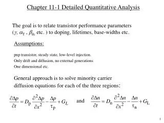
Chapter 11-1 Detailed Quantitative Analysis The goal is to relate transistor performance parameters (, T , dc etc. ) to doping, lifetimes, base-widths etc. • pnp transistor, steady state, low-level injection. • Only drift and diffusion, no external generations • One dimensional etc. Assumptions: General approach is to solve minority carrier diffusion equations for each of the three regions: and
General Quantitative Analysis Under steady state and when GL= 0, and For the base in pnp, we are interested only in holes. The rigorous analysis is carried out in chapter 11, but we are going to take a more simplified approach.
Injection Efficiency : Base transport factor :aT =IC / IEP Collector to emitter current gain: aDC =aT g Collector to base current gain: bDC =aDC / (1 – aDC) Review: Operational Parameters IEP IBR –IEN –IBE –IBR
Review of P-N Junction Under Forward Bias + VEB nE(0) pB(0) P (emitter) N (base) Area = Qp Area = Qn pB0 nE0 xE xB 0 0
Review of P-N Junction Under Forward Bias (cont.) In = q A DE dn/dxE = – (q A DE/LE) nE(0) Ip= – q A DB dp/dxB = (q A DB/LB) pB(0) Total current I = IP +(– IN) (“–” because xE and xB point in opposite directions) = (q A DB/LB) pB(0) + (q A DE/LE) n E (0) = (q A DB/LB) pB0[exp (q VEB / kT) –1] + + (q A DE/LE) nE0[exp (q VEB /kT) –1] ≈(q A DB/LB) pB0 exp (q VEB/kT) + (q A DE/LE) nE0 exp (q VEB/kT) Note ! Ip and In can also be calculated based on the fact that Qp has to be replaced every B seconds Ip = Qp/B and In = Qn/E and IE = IP + IN
Emitter Base Collector pB(0) nE(0) nC0 pB0 nE0 nC(0) Simplified Analysis Consider the carrier distribution in a forward active pnp transistor
Simplified Analysis (cont.) nE0, pB0 and nC0 = equilibrium concentration of minority carriers in emitter, base and collector nE(0), pB(0)and nC(0) = minority carrier concentration under forward active conditions at the edge of the respective depletion layers nE (0), pB(0)and nC(0) = Excess carrier concentration at the edge of the depletion layers
Simplified Analysis (cont.) nE (0) = nE (0) – nE0 = nE0 [exp (q VEB / kT) – 1] pB (0) = pB (0) – pB0 = pB0 [exp (q VEB / kT) – 1] By taking the slopes of these minority carrier distribution at the depletion layer edges and multiplying it by “qAD”, we can get hole and electron currents. Note that In = q A Dn (dn/dx) and Ip = – q A Dp (dp / dx)
Calculation of Currents • Collector current, IC • Ic = q A DB (dp/dxB) (slope must be taken at end of base) • = q A DB [pB(0) – 0] / WB • = q A DB pB(0) / WB • Ic = q A (DB/WB) pB0 exp (qVEB / kT)---- (A) • (only hole current if we neglect the small reverse saturation current of reverse biased C-B junction)
Calculation of Currents (cont.) • Emitter Current, IE • IE is made up of two components, namely IEP and IEN • IEP = Ic + current lost in base due to recombination • = Ic + excess charge stored in base/B • = Ic + q A WBpB(0) / (2B) • q A (D B/W B) pB0 [exp (qVEB / kT) ] • + q A [W B/(2B)] pB0 [exp (qVEB / kT)] --- (B) • [ Assuming exp (qVEB / kT) – 1 exp (qVEB / kT) • when VEB is positive, i.e forward biased. ]
Calculation of Currents (cont.) • Emitter Current (cont.) • IEN corresponds to electron current injection from base to emitter since E-B junction is forward biased. • IEN = qA (D E / LE) nE0 [exp (q VEB / kT) – 1 ] • qA (D E / LE) nE0 [exp (q VEB / kT)] ----- (C)
Calculation of Currents (cont.) • Base Current, IB • supplies electrons for recombination in base • supplies electrons for injection to emitter. • IB = qA pB0 [WB / (2B )] [exp (qV EB / kT) ] • + • qA(D E / LE) nE0 exp (qV EB / kT) • ( recombination) + (electron injection to emitter) • Now we can find transistor parameter easily.
Calculation of Currents (cont.) Base transport factor, T T = IC / IEP (same as eq. 11.42 in text) Emitter injection efficiency, = IEP / [ IEP + IEN ] = 1 / [ 1 + IEN / IEP ] = 1 / [ 1+ (C) / (B)]
DC = DC / (1– DC ) Calculation of Currents (cont.) (Eq 11.41 in textbook) nE0 = ni2/ NE … doping in emitter pB0 = ni2/ NB … doping in base dc= T