Download
1 / 24
240 likes | 264 Vues
This research focuses on the development and testing of ultra-fast silicon detectors for high time resolution measurements. The study includes measurements, contributions to time resolution research, and R&D for the ATLAS HGTD by CSM.

E N D
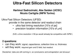
Ultra-Fast Silicon Detectors Hartmut F.-W. Sadrozinski SCIPP, Univ. of California Santa Cruz, CA 95064, USA for the UFSD Group UCSC – Torino – CNM Barcelona – IJS Ljubljana- LPNHE Hartmut F.-W. Sadrozinski, 75 um LGAD, "Trento" 2016 • First measurements on 75 um LGAD • Contributions to UFSD time resolution • R&D for ATLAS HGTD by CSM
LGAD Testing with source For the first beam tests we used commercial amplifiers with bias-T. For the next tests with 90Sr sources and beams, we developed a broadband amplifier (BW > 2GHz, discrete SiGe frontend, analog readout into digital scope) Signals in: LGAD, power, sensor bias Signals out: single-ended analog signals into 50 Ω Important: development of shielding Use source as test bed for signal and noise performance: tune the details of the circuit with LGAD data!. Precision measurements will be done in beam tests. Scintillator + SiPM (Trigger) Hartmut F.-W. Sadrozinski, 75 um LGAD, "Trento" 2016 LGAD Signal
LGAD detectors for HGTD Beam Test Expect by May 2016: 2x2 arrays of 3 mm and 2 mm side length various thickness and doping concentration (see later slides) Amplification and time digitization is required locally for trigger ASIC development just starting For the first beam tests plan to use broadband amplifier developed by UCSC 4 amplifier channels (~ 1mm width) wire-bonded to 2x2 array 2 mm Hartmut F.-W. Sadrozinski, 75 um LGAD, "Trento" 2016
Beam data with 75 um LGAD (G = ?) 75 um, ‘s Pulses shorter than simulation!? Ave. Time Jitter < 40ps Time Jitter: 11 ps Hartmut F.-W. Sadrozinski, 75 um LGAD, "Trento" 2016 Pulse shape suggests gain G ≈ 10! 300 um, CERN BT Filtered time resolution ~100ps Time Jitter: ~ 200 ps
dV/dt Comparison of 75 um - 300um LGAD 300um: 21 average used to reduce noise 1 ns shaping ≈ 1/3 of rise time Amplitude dV/dt High frequencies not important for 300um (Need to adjust the CFD threshold) High frequencies very important for 75um (only for BB) Hartmut F.-W. Sadrozinski, 75 um LGAD, "Trento" 2016 Amplitude dV/dt 75um: 21 averages reduces dV/dt by ½ 500 ps shaping ≈ rise time Fast, low-noise amplifier a requirement
C-V 50um (W8) & 75um (W11) epi LGAD Run 6827 50um: C-V suggests gain G < 3! also measured Hartmut F.-W. Sadrozinski, 75 um LGAD, "Trento" 2016 75um: C-V suggests gain G > 10! 300um: measured gain G > 10!
Toward LGAD Specifications for HGTD Larger cell size, higher gain, lower resistivity (?) ==> increased shot noise, Larger cell size ==> increased electronic noise (CSA), lower dV/dt (BB) Thicker sensors ==> increased Landau Noise Lower input impedance ==> lower trans-impedance Electronics and sensors are closely coupled. Both LGAD and no-gain n-in-p are being considered To get to 10 ps jitter: dV/dtat threshold > 0.5 uV/ps? Noise (into 50Ohm) < 5 uV ? LGAD details (all numbers TBD): Gain 10 - 20 Thickness <100 um Resistivity 0.1 - 10 kΩ-cm Cell size dimension 2-5 mm Impedance at amplifier input 20 – 50 Ω Radiation Hardness (Leakage current,Noise, dV/dt) Power per cell Power per cm^2 Hartmut F.-W. Sadrozinski, 75 um LGAD, "Trento" 2016
Jitter • Time Jitter = Noise/slope = Noise / (dV/dt) • Hard to predict the noise in the moment. • At least we know that for BB it is constant vs capacitance. • Need to know what it is as a function of the input impedance. • (Data taken with amplifier with gain = 130 shows 4uV at 1 GHz.) Hartmut F.-W. Sadrozinski, 75 um LGAD, "Trento" 2016
Slew-rate (Slope) dV/dt Assume that the resolution scales with slope dV/dt. For 50um LGAD (G=10), required dV/dt = 0.7 uV/ps(correcting for gain = 100 in WF2). Slope dV/dt = 0.5 uV/ps would give 40ps Hartmut F.-W. Sadrozinski, 75 um LGAD, "Trento" 2016
Bulk Resistivity • Resistivity 0.1 - 10 kΩ-cm • Low-resistivity bulk (100 Ω-cm) generates high field at the junction • (about ½ what is needed for LGAD). • Only half needs to be supplied by p+ multiplication layer Hartmut F.-W. Sadrozinski, 75 um LGAD, "Trento" 2016 Observe remarkable bias reach in low-resistivity LGAD We are operating 50um & 70um epi sensors with 100 Ω-cm bulk at 650 V bias.
E-field in LGAD bulk adds to the “gain field” Low-resistivity bulk (100 Ω-cm) generates high field at the junction (about ½ what is needed for LGAD). Only 1/2 is supplied by p+ multiplication layer Hartmut F.-W. Sadrozinski, 75 um LGAD, "Trento" 2016 Near-term: thin 4” wafers at CNM SOI 100um & 150um > 5kΩ-cm Epi 50um 100Ω-cm; 75um 100Ω-cm; 110um 600Ω-cm
Landau Fluctuations • Beam Tests show that we can correct for time walk. • So assuming we can beat the time jitter with lower noise and higher gain, Landau fluctuations become the time resolution floor which we can’t go below. • They depend on the sensors thickness, independent of the gain. • Both thin sensors, and low threshold are required for good timing resolution: • Another reason to develop low- noise amplifiers Hartmut F.-W. Sadrozinski, 75 um LGAD, "Trento" 2016
Cell Size • Cell size dimension 2-5 mm • Need gain, need small detector sizes to get to sufficient dV/dtInto 50Ω Hartmut F.-W. Sadrozinski, 75 um LGAD, "Trento" 2016
Impedance at Amplifier Input 20 – 50Ω Lowering the amplifier input impedance allows higher slope dV/dt. We need to assertain that the noise scales exactly, too. Hartmut F.-W. Sadrozinski, 75 um LGAD, "Trento" 2016
WF2 Simulation: Radiation Damage (Trapping) Effect of trapping in thick and thin detectors at large fluences is different since the trapping distance is ~ 50 µm. Effect of trapping: gain holes disappear, looks like a change in gain 300µm, Gain=10 The rising edge of thin sensors is essentially insensitive to trapping: good for timing! Hartmut F.-W. Sadrozinski, 75 um LGAD, "Trento" 2016 Trapping: Degradation of pulse height in 4*1015neq/cm2 down to ~ 20% for 300 µm LGAD down to ~ 50% for 50 µm LGAD An additional effect resulting in a decrease in gain beyond trapping has been reported in 300 µm LGADs and is being investigated on 50 µm LGAD. Investigate restoring gain loss after irradiation with increasing the bias voltage. Pursue program to improve radiation tolerance by replacing Boron with Gallium. 50µm, Gain=10 Weightfield 2 (WF2) Implementation and Simulation: Bianca Baldassari
Sentaurus Simulations (Julie Segal, SLAC) LGAD #1 (low gain) 50um thick Current vs. Time for 1MIP @100V BiasNo radiation, 1e14, 5e14 LGAD #3 (high gain) 50um thickCurrent vs. Time for 1MIP @100V Biasno radiation, 1e14, 5e14 Hartmut F.-W. Sadrozinski, 75 um LGAD, "Trento" 2016 N.B. “1MIP” relates to the amount of charge is injected into the backside of the LGAD: maximum . Similar results are reported by many groups: TCAD works “right out of the box” We are now measuring LGAD which were irradiated with protons at Los Alamos and neutrons at Llubljana.
HGTD Simulation, Design and fabrication. Hartmut F.-W. Sadrozinski, 75 um LGAD, "Trento" 2016 G. Pellegrini, M. Carulla, S. Hidalgo, D. Flores, D. Quirion
Design of HGTD ATLAS LGAD • 3x3 mm2 and 2x2mm2 pads separated by 33um (optimized by simulation). • P-stop isolation. • 50um thick active area. Support wafer can be etched away leaving a mechanical structure for mounting the read out chip and wire bonding. • Each chip reads out 4 channels. • Gain is set by the thickness of the substrate (max bias expected 200V due to the planar junction breakdown), a complete (technological and electrical) simulation has been performed using Sentaurus and Silvaco to find the parameter necessary for the fabrication. Expected gain 6-10 • Fabrication steps are the same than standards LGAD (with the thermal steps and implant energy and dose to be optimized by simulation). • First fabrication in 4” SOI wafers. Fabrication started in February 2016, wafers should be ready by May 2016. • Then fabrication should be optimized in 6” wafers. At the moment CNM is already doing a run of LGAD detectors in 6” wafers, 200um thick. The run is due in 2016. • Open question: are they radiation hard? Fluences expected up to 5x10E15neq/cm2. Hartmut F.-W. Sadrozinski, 75 um LGAD, "Trento" 2016
Core Structure passivation FE Multiplication dopant implant as measured by SIMS. The fabrication process is the same as for the standard 300um thick wafers. SiO2 n+ 30um p- 3000um 50um p+ p-stop p++ Hartmut F.-W. Sadrozinski, 75 um LGAD, "Trento" 2016 Al Al 50um 300um Electric Field @ 140V Wet etching of silicon
I-V Characteristics of thin detectors Beware of the dimensions of the active volume 50um epi Hartmut F.-W. Sadrozinski, 75 um LGAD, "Trento" 2016 Run 6474 300um FZ 75um epi 20
Transient Simulations and Measurements Hartmut F.-W. Sadrozinski, 75 um LGAD, "Trento" 2016
CNM Wafer Layout A1=8x8 matrix, 3mm pad B1=8x8 matrix, 2mm pad A2=4x4 matrix, 3mm pad B2=4x4 matrix, 2mm pad A3=2x2 matrix, 3mm pad B3=2x2 matrix, 2mm pad A4=2x2 matrix, 3mm pad, PIN B4=2x2 matrix, 2mm pad, PIN C=CT-PPS D=TOTEM detector Different diodes and test structures. Hartmut F.-W. Sadrozinski, 75 um LGAD, "Trento" 2016 3x3mm2 pixels. Hole in the metallization JTE only in the guard ring. P-stop isolation.
Contributors A. Anker, J. Chen, V. Fadeyev, P. Freeman, Z. Galloway, B. Gruey, H. Grabas, L.Hibbard, C. Labitan, Z. Liang, R. Losakul, S. N. Mak, C. W. Ng, Hartmut F.-W. Sadrozinski, A. Seiden, N. Woods, A. ZatserklyaniySCIPP, Univ. of California Santa Cruz, CA 95064, USA B. Baldassarri, N. Cartiglia, F. Cenna, M. Ferrero Univ. of Torino and INFN, Torino, Italy G. Pellegrini, S. Hidalgo, M. Baselga, M. Carulla, P. Fernandez-Martinez, D. Flores, A. Merlos, D. Quirion Centro Nacional de Microelectrónica (CNM-CSIC), Barcelona, Spain Hartmut F.-W. Sadrozinski, 75 um LGAD, "Trento" 2016
Conclusions • We took data in a triggered source with 75um thick epi LGAD with gain G ≈ 10 and measured a jitter of less than 40 ps. • The timing resolution in beam and laser tests are confirmed by the Weightfield 2 simulations. • We are developing specifications for LGAD to be used in the ATLAS HGTD. • We are looking forward to the next production run of UFSD at CNM available in May 2016. • Thanks to the organizers for arranging this year’s “Trento” meeting in Paris! Hartmut F.-W. Sadrozinski, 75 um LGAD, "Trento" 2016