Innovative Methods for the Synthesis and Fabrication of Graphene Sheets and Nanoribbons
This document outlines cutting-edge techniques for synthesizing graphene sheets and nanoribbons, including a focus on bottom-up technology as explored by Toshitake Takahashi and others. It discusses several fabrication methods such as the peel-off method, epitaxial growth, and a novel approach for large-scale applications. Furthermore, the electrical properties of graphene nanoribbons (GNR) in relation to their width, as well as their performance in vacuum and air environments, are examined. These findings provide significant insights into the future of graphene applications in electronics.

Innovative Methods for the Synthesis and Fabrication of Graphene Sheets and Nanoribbons
E N D
Presentation Transcript
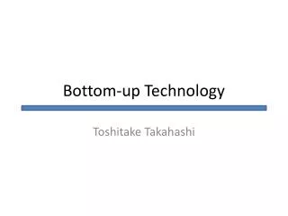
Bottom-up Technology Toshitake Takahashi
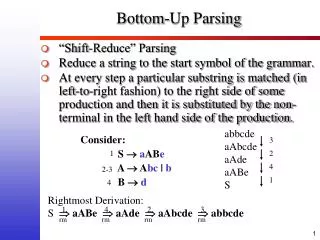
A B C Exfoliate PmPV Suspension in DCE solvent E D Centrifuge Background on the synthesis of graphene sheet and graphenenanoribbon Fabrication method so far • - Peel-off method • Epitaxial growth • Chemically Required new approach for Large scale application K. S. Novoselov, et al. Science 2004, 306, 666. Li, X. L. et al. Science 319, 1229–1232 (2008) W. A. de Heer, et. al. Science 2006, 312, 1191.
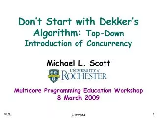
Making GNR from MWCNT • - PMMA- MWCNT film was peeled off in KOH solution • Top side wall of MWCNT were etched faster and • removed by plasma
Diameter/Width/Height distribution Diameter distribution of pristine MWCNT Width and height distribution of GNR
Electrical property of GNR 7 nm-wide GNR device measured in air • p-type behavior due to • Physisorbed O2 16 nm-wide GNR device measured in vacuum • After electrical annealing • Symmetric electron and hole • transport
Electrical characteristic of GNR • Transfer characteristic is strongly dependent on width • Opening of bandgap due to enhanced carrier confinement • and edge effect as GNR width is reduced