Download
1 / 22
220 likes | 367 Vues
A complete DC/DC converter ASIC for LHC upgrades. S. Michelis, F. Faccio , G . Blanchot , I. Troyano CERN PH-ESE S.Saggini University of Udine, Italy Twepp 2012, Oxford 17-21 September 2012. 1. Power distribution with DC-DC converters. Buck Converter Specifications: Vin<=10V

E N D
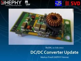
A complete DC/DC converter ASICfor LHC upgrades • S. Michelis, F. Faccio, G. Blanchot, I. Troyano • CERN PH-ESE • S.Saggini • University of Udine, Italy • Twepp 2012, Oxford 17-21 September 2012 1
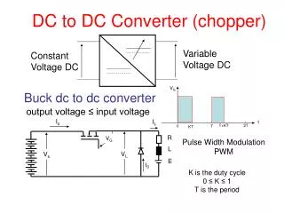
Power distribution with DC-DC converters • Buck Converter • Specifications: • Vin<=10V • Vout=1.2-3.3V • Iout<=3A • frequency=1-3 MHz • Constrains: • magnetic (2T-4T) fields • radiation (TID>100Mrd, • fluence > 2 1015 p/cm² • ions with LET<40MeV·cm²/mg) DC/DC ASIC 2
aMis 5 3
2.88mm 2.7 mm AMIS5 is designed in a High Voltage 0.35um technology for automotive application. This technology has been successfully tested for TID, protons and heavy ions. 4
Buffer / Drivers Analog Linear regulators High Side transistors Control Circuit Low Side transistors Digital Lin. Regulator capacitors 5
Buffers Two AMIS5 versions have been submitted (same dimension, same pinout) • BOSH • (Buffer Overcurrent=Small High) • slower turn on&off of power transistors • Over-Current detection on High Side Transistor • BOLL • (Buffer Overcurrent=Large Low) • faster turn on&off of power transistors • Over-Current detection on Low Side Transistor 6
AMIS5 Enable External Pull-up Voltage (<3.3V) Internal Enable 0.7V RExt Power Good ENABLE POWER GOOD • Power Good: is an open drain pin. • Power Good goes high if: • AMIS5 is enabled, Vin>5V and it is working properly • Power Good goes low (zero) when AMIS5 is supplied (Vin>5V) and if it is in one of these conditions: • Start-up • Over-Current limitation • Over-Temperature limitation • AMIS5 disabled • the ASIC is OFF by default • the Enable pin need to be externally controlled. • AMIS5 turn on if Venable>0.7V (compatible with 1.2V logic up to 3.3V) 8
ENABLE Half Swith Only 2/5th of the power transistors are operative. Higher efficiency for small load (<1A) 9
5V 4V Vin Vin Enabler for the converter converter off converter on Threshold Input Under – Voltage Protection Vin time (s) converter off 10
converter on 60°C 100°C converter off Over-Temperature Protection Temperature time (s) converter on 11
AMIS5 Efficiency with Vin=10V, L=460nH, Vout=2.5V, f=1.7MHz 13
Line and Load regulation @ f=1.7MHz, L=460nH Iout=3A Iout=2.5A Iout=2A Iout=1.5A Iout=0A Iout=1A Iout=0.5A Line regulation: 4mV variation with Vin=6V-12V Load regulation: 7mV variation with Iout=0A-3A 15
Load Transient Load transient setup thanks to Cristian Fuentes
TID tests pre-rad with Vin=10V, L=460nH, Vout=2.5V, f=1.7MHz 17
TID Tests at different temperature pre-rad with Vin=10V, L=460nH, Vout=2.5V, f=1.7MHz 18
Line and Load regulations vs TID with Vin=10V, L=460nH, Vout=2.5V, f=1.7MHz pre-rad 19
Future plans • Test foreseen for AMIS5 Single Event and Displacement damage tests (fall 2012) BOSH version tests Tests on AMIS5 packaged in QFN32 • AMIS5_BB Bump Bonded version tests and characterization (expected back in November 2012) AMIS5_BB 3.3 mm 2.88mm 20
Negative Converter 21
13.5 mm Differential Mode noise Positive Converter Differential Mode noise Negative Converter 28.5 mm Negative Converter Positive Converter Board designed by Isaac Troyano Vin Phase Vout DC/DC For the time being the DC/DC converter is a commercial chip (LTC3605, the same for SM01C). It will be replaced with AMIS5 -Vout 22
Conclusions • A new DC/DC converter ASIC called AMIS5 has been presented. It is a fully integrated synchronous buck converter which contains internal linear regulators, bandgaps and a control circuitry to handle signals form the protection circuitry Efficiency is high (above 80%, peak 83%-85%) Radiation effects are limited (2-4% loss of efficiency over 325Mrad and Iout=2-3A) line regulation is good (4 mV for Vin variation from 6 to 12V) load regulation is good (7 mV for Iout variation from 0 to 3A) • A negative converter has been presented It allows to convert a positive input voltage to a negative voltage (e.x. Vin=7V and Vout=-2.5V). It uses a chip that has been already used for a positive convert. Only the PCB layout is changed. AMIS5 will replace the commercial component for radiation tolerance 23