Download
1 / 1
20 likes | 259 Vues
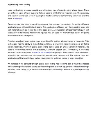
ADVANCED LASER CUTTING OF ELECTRONIC SUBSTRATES. Tran Thi Ngoc Phuong (NUS High School of Math and Science) & Axel Chu Jun Ming (St Andrew’s Junior College) Supervisor : Dr. Wang Xincai (SiMTech). Cutting edges of polyimide substrate. Laser cutting on pure polyimide substrate.

E N D
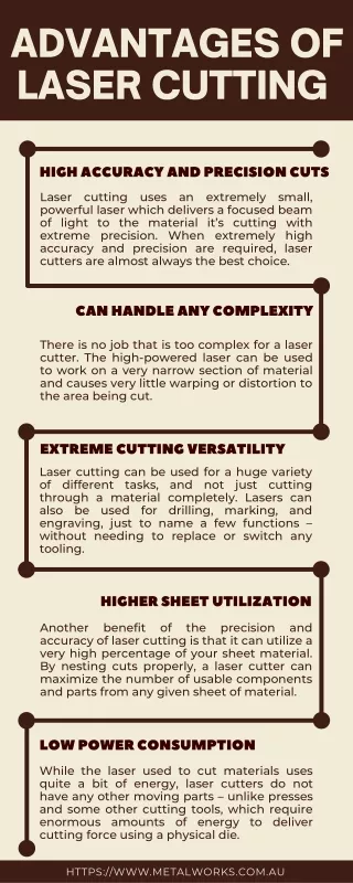
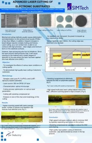
ADVANCED LASER CUTTING OF ELECTRONIC SUBSTRATES Tran Thi Ngoc Phuong (NUS High School of Math and Science) & Axel Chu Jun Ming (St Andrew’s Junior College) Supervisor : Dr. Wang Xincai (SiMTech) Cutting edges of polyimide substrate Laser cutting on pure polyimide substrate Laser cutting on Cu/PI/Cu Laser cutting on Cu/PI/Cu Laser cutting on Cu/BT-epoxy/Cu Introduction Mechanical cutting methods usually causes deformation and delamination on thin printed circuit boards (PCBs) of less than 300μm, In addition, frequent changes in board design requires complex tooling and fixtures. Laser cutting, as a non-contact tool, is able to cut contours with high precision, clean edges and minimum burrs on the substrate surfaces. However, laser processing also has its limitations. Since the laser process itself produces heat, it will cause charring on the material and a certain degree of distortion to the area where the laser has been applied. (the heat affected zone (HAZ) ). • As repetition rate increased, the power increased up to a maximum at 40kHz • At low repetition rate (10kHz), the cutting edge was observed to be crooked. • Objective • To investigate the effects of various laser conditions on cutting quality • To demonstrate high quality laser cutting of electronic substrates Fig 2 Average power (W) versus Repetition rate (kHz) • Methodology • Samples used: pure PI, Cu/PI/Cu and Cu/BT-epoxy/Cu based substrates • Laser source: 355 nm DPSS UV laser • Characterization: optical microscope • Cutting process optimization on various laser parameters • Cutting with assisting compressed air • Analysis on size of the char and morphology of the cutting - Assisting compressed air effectively reduced the HAZ on polyimide substrate (fig 3) Fig 3 Laser cutting with assisting compressed air - High speed multi-pass laser cutting helped reduce the HAZ. (effective scanning speed is kept constant) (Fig 4) • Results • Higher scanning speed with same average power, number of passes and repetition rate reduces heat affected zone (Fig 1) (a) (b) (c) Fig 4 Laser cutting on pure polyimide substrate with repetition rate of 40kHz, average power output of 10W, scanning speed of (a) 100m/s for 1 pass (b) 500m/s for 5 passes and (c) 2000m/s for 20 passes • Conclusion • High speed multi-pass cutting is able to minimize HAZ by spatially separating each pulse on the surface. • Assisting compressed air can help to reduce the HAZ and charring. • High quality laser pattern cutting of electronic substrates was demonstrated as shown in the top pictures. (a) (b) (c) Fig 1 Laser cutting on pure polyimide substrate with repetition rate of 40kHz, average power output of 10W, scanning speed of (a) 200m/s for 1 pass (b) 300m/s for 1 pass and (c) 500m/s for 1 pass