Microcomputer Buses
Outline What is a Bus? Interfaces Open Collector Buses Tristate Buses Bus Contention Transmission Lines Goal Understand bus basics Understand bus analysis Reading Microprocessor Systems Design, Clements, Ch. 10. Microcomputer Buses. Bus functions distribute power distribute clocks

Microcomputer Buses
E N D
Presentation Transcript
Outline What is a Bus? Interfaces Open Collector Buses Tristate Buses Bus Contention Transmission Lines Goal Understand bus basics Understand bus analysis Reading Microprocessor Systems Design, Clements, Ch. 10 Microcomputer Buses
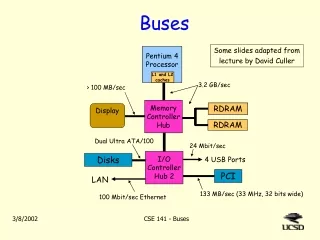
Bus functions distribute power distribute clocks data transfer Standards mechanical electrical protocol Challenges cheap - use few wires fast - over long distances good - plug-and-play What is a Bus?
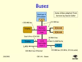
Dominant cost factor Minimal performance factor Band/blade connector gold-plated fingers on edge of PCB push into socket with spring-loaded fingers cheap, but unreliable, low density, board must be vertical today used for daughter cards, e.g. memory modules Socket connector half of socket on bus backplane, half on board pin connections reliable, dense, more expensive, variety of orientations used for larger daughter cards, system bus, etc. Mechanical Interfaces
Goal - transmit signals fast and reliably Bus drivers convert logic level to standard electrical signal drive on bus must avoid bus contention - driver fighting Bus receivers receive standard signal, convert to logic level fast, noise immune, low bus loading Bus wire transmission characteristics ideally just a capacitor really a messy transmission line reflections coupling to neighboring lines presence/absence of cards changes characteristics Electrical Interface
Must maintain proper voltage and current levels VOH/VOL - output high/low voltage VIH/VIL - input high/low voltage IOH/IOL - output high/low current (positive means sink) IIH/IIL - input high/low current (negative means source) DC noise immunity high-level voltage immunity = VOH - VIH low-level voltage immunity = VIL - VOL the larger, the better for noise, but can reduce speed bus drivers and receivers must agree on logic 0/1 levels Bus Drivers/Receivers
Bus driver must be able to source/sink sufficient current e.g. source 20 uA, sink 0.4 mA for every LS TTL input driven maintains DC logic values Current drive must be much higher to achieve speed driving large capacitance of bus 75 MHz, 10 100 pF loads, 5V, 50% margin => 750 mA receiver design tries to minimize capacitance use standard receivers at card interface shield internal card capacitance provide standard load but cause additional delay Current Levels
How to hook multiple drivers to bus standard TTL or CMOS will fight if driving both 0 and 1 most standard logic will burn out Solution: passive drivers can only pull bus down use resistor to pull bus up open collector driver open drain in CMOS/NMOS technology wired OR - any driver can pull down bus to logic 0 Passive Drivers
Conflicting requirements maximum value that will keep logic 1 on bus minimum value for speed, driver sink capability Maximum keep VOH with m drivers, n receivers Ileakage for drivers = 250 uA for LS TTL IIL for receivers = 20 uA for LS TTL noise margin = 0.4V VIH = 2.0V for LS TTL => VOH = 2.4V assume 10 drivers, 10 receivers Rmax = (Vcc - 2.4V)/(10*250uA+10*20uA) = 1000 ohms Resistor Design
Minimum value single driver must be able to achieve VOL VOL = 0.4V for 0.4V margin since VIL = 0.4V IIL = 0.4 mA IOL = 16 mA no driver leakage current assume 10 receivers Rmin = (Vcc - VOL)/(IOL - n*IIL) = 300 ohms Speed assume 100 pF per driver/receiver 10 driver/receivers => 1000 pF load delay ~ 2*R*C = 0.6-2 us => really slow Power 128 address/data lines * 5*(5-0.4)/300 = 9.8 W assume half of lines are high => ~5 W Resistor Design (cont.)
Driver has three states logic 0, logic 1, high impedance usually inverter or buffer with extra enable line Most common type of driver Transceiver driver pairs in opposite directions, separate enable lines driver in one direction acts as receiver use for bidirectional interfaces Buffer control need to control enable of drivers tricky for bidirectional buses tristate unless in use Tristate Drivers
Static contention only one driver in each logical state Dynamic contention timing delays cause driver A switches on before drive B is off Example read-after-write bus cycle CPU had data bus drivers on for write memory turns on data bus drivers for read Must examine logic and timing diagrams for all situations switching driver source Bus Contention
40 MHz 68030 write to read transition buffered AS* controls data bus drivers can ignore receivers Analysis tseparation = delay between driver A off, driver B on positive means no overlap tSH - min. AS* negation time tHL/tLH - min. high-to-low/max. low-to-high AS* buffer delay tOFF/tON - max. driver off/min. driver on delay assume LS TTL tseparation = tSH - tLH - tOFF + tHL + tON = 18 - 18 - 25 + 9 + 12 = -4 ns too slow, try FAST TTL tseparation = tSH - tLH - tOFF + tHL + tON = 18 - 5.2 - 6.5 + 2.5 + 3.5 = 12.3 ns Bus Contention Analysis
As speeds get faster, everything becomes analog If signal rise time < 2.5*wirelength/velocity, model as transmission line signal velocity ~5 ns/m in PCB trace example: Tr = 50 ps => trace > 0.4 cm is transmission line if rise time > 5*propagation delay, model wire as capacitor NOTE: Clements terminology is confusing, use the rules here Model bus as transmission lines model as distributed or lumped R, C, L elements signal velocity is sqrt(LC) per length typically 30-50% of light speed can be 10-20 ns/m in heavily-loaded bus Characteristic impedance Zo = sqrt(L/C) step voltage on input sees impedance V/Zo current flows into line Transmission Lines
Current in line hits terminating resistance RT can generate a reflecting voltage pulse reflections can be a large fraction of voltage pulse if RT = Zo, then no reflection - a matched impedance if no termination, reflect full voltage pulse back Reflections at both ends voltage at end point is series of steps causes delay and noise Termination try to terminate transmission line with matched impedance problem: hard to know or control bus impedance problem: multiple termination points Reflections
PCB has Zo ~ 100 ohms but connecting 100 ohm resistor to Vdd or Gnd reduces noise margin on bus Solution split termination to Vdd and Gnd 194 ohm equivalent impedance causes ~30% voltage reflection Active termination use voltage regulator with termination resistors Custom bus driver chips usually include internal termination But still big headache in high-speed systems killed the DECsystem-20/80 Terminations
Solution 1 allow time for reflections to die away e.g. wait extra time after signals are “valid” use matched impedance at ends of bus use ~100 ohms for PCB wires lightly load bus and avoid long stubs stub is side path at T junction problem: hard to do in big, high-speed design Solution 2 buy off-the-shelf bus explains popularity of standard motherboards Bus Design