Memory Hierarchies
Memory Hierarchies. Memory (as we’ve viewed it thus far). Big array of storage with more complex ways of indexing than registers Build addressing modes to support efficient translation of software abstractions Uses less space in instruction than 32-bit immediate field


Memory Hierarchies
E N D
Presentation Transcript
Memory (as we’ve viewed it thus far) Big array of storage with more complex ways of indexing than registers • Build addressing modes to support efficient translation of software abstractions • Uses less space in instruction than 32-bit immediate field A[i]; use base (i) + displacement (A) (scaled?) a.ptr; use base (a) + displacement (ptr)
Other Memory Issues What is the size of each element in memory? 0x000 0-255 Byte Half word Word 0x000 0 - 65535 0 - ~4B 0x000 Ignore 64-bit architectures for now, but know that they exist,and are the present/future
Points to most significant byte Points to least significant byte 0x000 11 0x000 FF 44 88 88 44 FF 11 Other Memory Issues Big-endian or Little-endian? Store 0x114488FF Big Endian easier: even though Intel is Little Endian, we’ll stick to big
SRAM vs. DRAM • SRAM (static random access memory) • Faster than DRAM • Each storage cell is larger, so smaller capacity for same area • 2-10ns access time • DRAM (dynamic random access memory) • Each storage cell tiny (capacitance on wire) • Can get 2GB chips today • 50-70ns access time • Leaky – need to periodically refresh data • What happens on a read? • CPU clock rates ~0.2ns-2ns (5GHz-500MHz)
column address column address sense amplifiers (row buffer) write back row address precharge Non-Uniform DRAM Access
Modern DRAMs • Add internal banking for parallelism • Can be in process of performing ops on more than one bank • Pipelined, synchronous interface allows this • Rambus uses high memory clock rate, narrower channels, and fixed packet lengths sense amps possibly shared among adjacent banks
IRAM/PIM? • Logic in DRAM process is slow • DRAM in logic process makes each bit larger • Probably never will be part of GP architectures • Part of BlueGene/L • Good for gaming chips(note that BOTH use embedded processors!)
L1 Cache (several KB) L2 Cache (½-32MB) Memory (128MB – fewGB) Disk (Many GB) Millions cycle access! Cache Design 101 Memory pyramid Reg 100s bytes 1 cycle access (early in pipeline) 1-3 cycle access L3 becoming more common(sometimes VERYLARGE) 6-15 cycle access 50-300 cycle access These are rough numbers: mileage may vary for latest/greatestCaches USUALLY made of SRAM
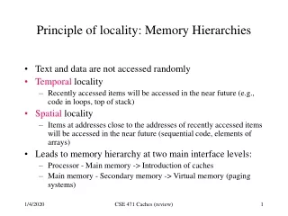
Terminology • Temporallocality: • If memory location X is accessed, then it is more likely to be re-accessed in the near future than some random location Y • Caches exploit temporal locality by placing a memory element that has been referenced into the cache • Spatial locality: • If memory location X is accessed, then locations near X are more likely to be accessed in the near future than some random location Y • Caches exploit spatial locality by allocating a cache line of data (including data near the referenced location)
A Simple Cache Processor Cache Memory 2 cache lines 3 bit tag field 2 byte block 0 1 2 3 4 5 6 7 8 9 10 11 12 13 14 15 100 110 120 Ld R1 M[ 1 ] Ld R2 M[ 5 ] Ld R3 M[ 1 ] Ld R3 M[ 4 ] Ld R2 M[ 0 ] 130 tag data 140 V 150 160 V 170 180 190 200 R0 R1 R2 R3 210 220 230 240 250
1st Access Processor Cache Memory 0 1 2 3 4 5 6 7 8 9 10 11 12 13 14 15 100 110 120 Ld R1 M[ 1 ] Ld R2 M[ 5 ] Ld R3 M[ 1 ] Ld R3 M[ 4 ] Ld R2 M[ 0 ] 130 tag data 140 0 150 160 0 170 180 190 200 R0 R1 R2 R3 210 220 230 240 250
Addr: 0001 1st Access Processor Cache Memory 0 1 2 3 4 5 6 7 8 9 10 11 12 13 14 15 100 110 120 Ld R1 M[ 1 ] Ld R2 M[ 5 ] Ld R3 M[ 1 ] Ld R3 M[ 4 ] Ld R2 M[ 0 ] 130 tag data 140 1 0 100 150 110 160 lru 0 170 180 block offset 190 200 R0 R1 R2 R3 210 110 220 Misses: 1 Hits: 0 230 240 250
2nd Access Processor Cache Memory 0 1 2 3 4 5 6 7 8 9 10 11 12 13 14 15 100 110 120 Ld R1 M[ 1 ] Ld R2 M[ 5 ] Ld R3 M[ 1 ] Ld R3 M[ 4 ] Ld R2 M[ 0 ] 130 tag data 140 1 0 100 150 110 160 lru 0 170 180 190 200 R0 R1 R2 R3 210 110 220 Misses: 1 Hits: 0 230 240 250
2nd Access Processor Cache Memory 0 1 2 3 4 5 6 7 8 9 10 11 12 13 14 15 100 110 120 Ld R1 M[ 1 ] Ld R2 M[ 5 ] Ld R3 M[ 1 ] Ld R3 M[ 4 ] Ld R2 M[ 0 ] 130 tag data 140 lru 1 0 100 150 110 160 1 2 140 170 150 180 block offset 190 Addr:0101 200 R0 R1 R2 R3 210 110 220 Misses: 2 Hits: 0 150 230 240 250
3rd Access Processor Cache Memory 0 1 2 3 4 5 6 7 8 9 10 11 12 13 14 15 100 110 120 Ld R1 M[ 1 ] Ld R2 M[ 5 ] Ld R3 M[ 1 ] Ld R3 M[ 4 ] Ld R2 M[ 0 ] 130 tag data 140 lru 1 0 100 150 110 160 1 2 140 170 150 180 block offset 190 Addr:0001 200 R0 R1 R2 R3 210 110 220 Misses: 2 Hits: 0 150 230 240 250
3rd Access Processor Cache Memory 0 1 2 3 4 5 6 7 8 9 10 11 12 13 14 15 100 110 120 Ld R1 M[ 1 ] Ld R2 M[ 5 ] Ld R3 M[ 1 ] Ld R3 M[ 4 ] Ld R2 M[ 0 ] 130 tag data 140 1 0 100 150 110 160 lru 1 2 140 170 150 180 190 200 R0 R1 R2 R3 210 110 220 Misses: 2 Hits: 1 150 230 110 240 250
4th Access Processor Cache Memory 0 1 2 3 4 5 6 7 8 9 10 11 12 13 14 15 100 110 120 Ld R1 M[ 1 ] Ld R2 M[ 5 ] Ld R3 M[ 1 ] Ld R3 M[ 4 ] Ld R2 M[ 0 ] 130 tag data 140 1 0 100 150 110 160 lru 1 2 140 170 150 180 block offset 190 Addr:0100 200 R0 R1 R2 R3 210 110 220 Misses: 2 Hits: 1 150 230 110 240 250
4th Access Processor Cache Memory 0 1 2 3 4 5 6 7 8 9 10 11 12 13 14 15 100 110 120 Ld R1 M[ 1 ] Ld R2 M[ 5 ] Ld R3 M[ 1 ] Ld R3 M[ 4 ] Ld R2 M[ 0 ] 130 tag data 140 lru 1 0 100 150 110 160 1 2 140 170 150 180 190 200 R0 R1 R2 R3 210 110 220 Misses: 2 Hits: 2 150 230 140 240 250
5th Access Processor Cache Memory 0 1 2 3 4 5 6 7 8 9 10 11 12 13 14 15 100 110 120 Ld R1 M[ 1 ] Ld R2 M[ 5 ] Ld R3 M[ 1 ] Ld R3 M[ 4 ] Ld R2 M[ 0 ] 130 tag data 140 lru 1 0 100 150 110 160 1 2 140 170 150 180 block offset 190 Addr:0000 200 R0 R1 R2 R3 210 110 220 Misses: 2 Hits: 2 150 230 140 240 250
5th Access Processor Cache Memory 0 1 2 3 4 5 6 7 8 9 10 11 12 13 14 15 100 110 120 Ld R1 M[ 1 ] Ld R2 M[ 5 ] Ld R3 M[ 1 ] Ld R3 M[ 4 ] Ld R2 M[ 0 ] 130 tag data 140 1 0 100 150 110 160 lru 1 2 140 170 150 180 190 200 R0 R1 R2 R3 210 110 220 Misses: 2 Hits: 3 140 100 230 140 240 250
Basic Cache Organization Decide on the block size • How? Simulate lots of different block sizes and see which one gives the best performance • Most systems use a block size between 32 bytes and 128 bytes • Longer sizes reduce the overhead by • Reducing the number of tags • Reducing the size of each tag Tag Block offset
What about Stores? • Where should you write the result of a store? • If that memory location is in the cache? • Send it to the cache. • Should we also send it to memory right away?(write-through policy) • Wait until we kick the block out (write-back policy) • If it is not in the cache? • Allocate the line (put it in the cache)?(write allocate policy) • Write it directly to memory without allocation?(no write allocate policy)
Handling Stores (Write-Through) Processor Cache Memory 0 1 2 3 4 5 6 7 8 9 10 11 12 13 14 15 Assume write-allocate policy 78 29 120 123 Vtag data Ld R1 M[ 1 ] Ld R2 M[ 7 ] St R2 M[ 0 ] St R1 M[ 5 ] Ld R2 M[ 10 ] 71 0 150 162 0 173 18 21 33 R0 R1 R2 R3 28 19 Misses: 0 Hits: 0 200 210 225
Write-Through (REF 1) Processor Cache Memory 0 1 2 3 4 5 6 7 8 9 10 11 12 13 14 15 78 29 120 123 V tag data Ld R1 M[ 1 ] Ld R2 M[ 7 ] St R2 M[ 0 ] St R1 M[ 5 ] Ld R2 M[ 10 ] 71 0 150 162 0 173 18 21 33 R0 R1 R2 R3 28 19 Misses: 0 Hits: 0 200 210 225
Write-Through (REF 1) Processor Cache Memory 0 1 2 3 4 5 6 7 8 9 10 11 12 13 14 15 78 29 120 123 V tag data Ld R1 M[ 1 ] Ld R2 M[ 7 ] St R2 M[ 0 ] St R1 M[ 5 ] Ld R2 M[ 10 ] 71 78 1 0 150 29 162 lru 0 173 18 21 33 R0 R1 R2 R3 28 29 19 Misses: 1 Hits: 0 200 210 225
Write-Through (REF 2) Processor Cache Memory 0 1 2 3 4 5 6 7 8 9 10 11 12 13 14 15 78 29 120 123 V tag data Ld R1 M[ 1 ] Ld R2 M[ 7 ] St R2 M[ 0 ] St R1 M[ 5 ] Ld R2 M[ 10 ] 71 78 1 0 150 29 162 lru 0 173 18 21 33 R0 R1 R2 R3 28 29 19 Misses: 1 Hits: 0 200 210 225
Write-Through (REF 2) Processor Cache Memory 0 1 2 3 4 5 6 7 8 9 10 11 12 13 14 15 78 29 120 123 V tag data Ld R1 M[ 1 ] Ld R2 M[ 7 ] St R2 M[ 0 ] St R1 M[ 5 ] Ld R2 M[ 10 ] 71 lru 78 1 0 150 29 162 1 3 162 173 173 18 21 33 R0 R1 R2 R3 28 29 19 Misses: 2 Hits: 0 173 200 210 225
Write-Through (REF 3) Processor Cache Memory 0 1 2 3 4 5 6 7 8 9 10 11 12 13 14 15 78 29 120 123 V tag data Ld R1 M[ 1 ] Ld R2 M[ 7 ] St R2 M[ 0 ] St R1 M[ 5 ] Ld R2 M[ 10 ] 71 lru 78 1 0 150 29 162 1 3 162 173 173 18 21 33 R0 R1 R2 R3 28 29 19 Misses: 2 Hits: 0 173 200 210 225
173 173 Write-Through (REF 3) Processor Cache Memory 0 1 2 3 4 5 6 7 8 9 10 11 12 13 14 15 29 120 123 V tag data Ld R1 M[ 1 ] Ld R2 M[ 7 ] St R2 M[ 0 ] St R1 M[ 5 ] Ld R2 M[ 10 ] 71 1 0 150 29 162 lru 1 3 162 173 173 18 21 33 R0 R1 R2 R3 28 29 19 Misses: 2 Hits: 1 173 200 210 225
Write-Through (REF 4) Processor Cache Memory 0 1 2 3 4 5 6 7 8 9 10 11 12 13 14 15 173 29 120 123 V tag data Ld R1 M[ 1 ] Ld R2 M[ 7 ] St R2 M[ 0 ] St R1 M[ 5 ] Ld R2 M[ 10 ] 71 173 1 0 150 29 162 lru 1 3 162 173 173 18 21 33 R0 R1 R2 R3 28 29 19 Misses: 2 Hits: 1 173 200 210 225
29 29 Write-Through (REF 4) Processor Cache Memory 0 1 2 3 4 5 6 7 8 9 10 11 12 13 14 15 173 29 120 123 V tag data Ld R1 M[ 1 ] Ld R2 M[ 7 ] St R2 M[ 0 ] St R1 M[ 5 ] Ld R2 M[ 10 ] 71 lru 173 1 0 150 29 162 1 2 71 173 150 18 21 33 R0 R1 R2 R3 28 29 19 Misses: 3 Hits: 1 173 200 210 225
Write-Through (REF 5) Processor Cache Memory 0 1 2 3 4 5 6 7 8 9 10 11 12 13 14 15 173 29 120 123 V tag data Ld R1 M[ 1 ] Ld R2 M[ 7 ] St R2 M[ 0 ] St R1 M[ 5 ] Ld R2 M[ 10 ] 71 lru 173 1 0 29 29 162 1 2 71 173 29 18 21 33 R0 R1 R2 R3 28 29 19 Misses: 3 Hits: 1 173 200 210 225
Write-Through (REF 5) Processor Cache Memory 0 1 2 3 4 5 6 7 8 9 10 11 12 13 14 15 173 29 120 123 V tag data Ld R1 M[ 1 ] Ld R2 M[ 7 ] St R2 M[ 0 ] St R1 M[ 5 ] Ld R2 M[10 ] 71 1 5 33 29 28 162 lru 1 2 71 173 29 18 21 33 R0 R1 R2 R3 28 29 19 Misses: 4 Hits: 1 33 200 210 225
How Many Memory References? • Each miss reads a block (only two bytes in this cache) • Each store writes a byte • Total reads: eight bytes • Total writes: two bytes but caches generally miss < 20%usually much lower hit rates . . . but depends on app!
Write-Through vs. Write-Back We can also design the cache to NOT write all stores to memory immediately? • We can keep the most current copy in the cache and update the memory when that data is evicted from the cache (a write-back policy) • Do we need to write-back all evicted lines? • No, only blocks that have been stored into • Keep a “dirty bit”, reset when the line is allocated, set when the block is stored into. If a block is “dirty” when evicted, write its data back into memory
Handling Stores (Write-Back) Processor Cache Memory 0 1 2 3 4 5 6 7 8 9 10 11 12 13 14 15 78 29 120 123 Vdtag data Ld R1 M[ 1 ] Ld R2 M[ 7 ] St R2 M[ 0 ] St R1 M[ 5 ] Ld R2 M[ 10 ] 71 0 150 162 0 173 18 21 33 R0 R1 R2 R3 28 19 Misses: 0 Hits: 0 200 210 225
Write-Back (REF 1) Processor Cache Memory 0 1 2 3 4 5 6 7 8 9 10 11 12 13 14 15 78 29 120 123 V d tag data Ld R1 M[ 1 ] Ld R2 M[ 7 ] St R2 M[ 0 ] St R1 M[ 5 ] Ld R2 M[ 10 ] 71 0 150 162 0 173 18 21 33 R0 R1 R2 R3 28 19 Misses: 0 Hits: 0 200 210 225
Write-Back (REF 1) Processor Cache Memory 0 1 2 3 4 5 6 7 8 9 10 11 12 13 14 15 78 29 120 123 V d tag data Ld R1 M[1 ] Ld R2 M[ 7 ] St R2 M[ 0 ] St R1 M[ 5 ] Ld R2 M[ 10 ] 71 1 0 0 78 150 29 162 lru 0 173 18 21 33 R0 R1 R2 R3 28 29 19 Misses: 1 Hits: 0 200 210 225
Write-Back (REF 2) Processor Cache Memory 0 1 2 3 4 5 6 7 8 9 10 11 12 13 14 15 78 29 120 123 V d tag data Ld R1 M[ 1 ] Ld R2 M[7] St R2 M[ 0 ] St R1 M[ 5 ] Ld R2 M[ 10 ] 71 1 0 0 78 150 29 162 lru 0 173 18 21 33 R0 R1 R2 R3 28 29 19 Misses: 1 Hits: 0 200 210 225
Write-Back (REF 2) Processor Cache Memory 0 1 2 3 4 5 6 7 8 9 10 11 12 13 14 15 78 29 120 123 V d tag data Ld R1 M[ 1 ] Ld R2 M[7] St R2 M[ 0 ] St R1 M[ 5 ] Ld R2 M[ 10 ] 71 lru 1 0 0 78 150 29 162 1 0 3 162 173 173 18 21 33 R0 R1 R2 R3 28 29 19 Misses: 2 Hits: 0 173 200 210 225
Write-Back (REF 3) Processor Cache Memory 0 1 2 3 4 5 6 7 8 9 10 11 12 13 14 15 78 29 120 123 V d tag data Ld R1 M[ 1 ] Ld R2 M[ 7 ] St R2 M[0] St R1 M[ 5 ] Ld R2 M[ 10 ] 71 lru 1 0 0 78 150 29 162 1 0 3 162 173 173 18 21 33 R0 R1 R2 R3 28 29 19 Misses: 2 Hits: 0 173 200 210 225
Write-Back (REF 3) Processor Cache Memory 0 1 2 3 4 5 6 7 8 9 10 11 12 13 14 15 78 29 120 123 V d tag data Ld R1 M[ 1 ] Ld R2 M[ 7 ] St R2 M[0] St R1 M[ 5 ] Ld R2 M[ 10] 71 1 1 0 173 150 29 162 lru 1 0 3 162 173 173 18 21 33 R0 R1 R2 R3 28 29 19 Misses: 2 Hits: 1 173 200 210 225
Write-Back (REF 4) Processor Cache Memory 0 1 2 3 4 5 6 7 8 9 10 11 12 13 14 15 78 29 120 123 V d tag data Ld R1 M[ 1 ] Ld R2 M[ 7 ] St R2 M[ 0 ] St R1 M[5] Ld R2 M[ 10 ] 71 1 1 0 173 150 29 162 lru 1 0 3 162 173 173 18 21 33 R0 R1 R2 R3 28 29 19 Misses: 2 Hits: 1 173 200 210 225
Write-Back (REF 4) Processor Cache Memory 0 1 2 3 4 5 6 7 8 9 10 11 12 13 14 15 78 29 120 123 V d tag data Ld R1 M[ 1 ] Ld R2 M[ 7 ] St R2 M[ 0 ] St R1 M[5] Ld R2 M[ 10 ] 71 lru 1 1 0 173 150 29 162 1 1 3 71 173 29 18 21 33 R0 R1 R2 R3 28 29 19 Misses: 3 Hits: 1 173 200 210 225
Write-Back (REF 5) Processor Cache Memory 0 1 2 3 4 5 6 7 8 9 10 11 12 13 14 15 78 29 120 123 V d tag data Ld R1 M[ 1 ] Ld R2 M[ 7 ] St R2 M[ 0 ] St R1 M[ 5 ] Ld R2 M[10] 71 lru 1 1 0 173 150 29 162 1 1 3 71 173 29 18 21 33 R0 R1 R2 R3 28 29 19 Misses: 3 Hits: 1 173 200 210 225
Write-Back (REF 5) Processor Cache Memory 0 1 2 3 4 5 6 7 8 9 10 11 12 13 14 15 78 173 29 120 123 V d tag data Ld R1 M[ 1 ] Ld R2 M[ 7 ] St R2 M[ 0 ] St R1 M[ 5 ] Ld R2 M[10] 71 lru 1 1 0 173 150 29 162 1 1 3 71 173 29 18 21 33 R0 R1 R2 R3 28 29 19 Misses: 4 Hits: 1 173 200 210 225
Write-Back (REF 5) Processor Cache Memory 0 1 2 3 4 5 6 7 8 9 10 11 12 13 14 15 78 29 120 123 V d tag data Ld R1 M[ 1 ] Ld R2 M[ 7 ] St R2 M[ 0 ] St R1 M[ 5 ] Ld R2 M[10] 71 1 0 5 33 150 28 162 lru 1 1 3 71 173 29 18 21 33 R0 R1 R2 R3 28 29 19 Misses: 4 Hits: 1 33 200 210 225
How many memory references? • Each miss reads a block Two bytes in this cache • Each evicted dirty cache line writes a block • Total reads: eight bytes • Total writes: four bytes (after final eviction) Choose write-back or write-through?
Direct-Mapped Cache Memory Address 01011 Cache 00000 00010 00100 00110 01000 01010 01100 01110 10000 10010 10100 10110 11000 11010 11100 11110 V d tag data 78 23 29 218 0 120 10 0 123 44 0 71 16 0 150 141 162 28 173 214 Block Offset (1-bit) 18 33 21 98 Line Index (2-bit) 33 181 28 129 Tag (2-bit) 19 119 200 42 210 66 Compulsory Miss: First reference to memory block Capacity Miss: Working set doesn’t fit in cache Conflict Miss: Working set maps to same cache line 225 74