Download
1 / 22
220 likes | 381 Vues
First test results with the Gigabit Link Interface Board (GLIB) Paschalis VICHOUDIS CERN PH-ESE-BE on behalf of the GLIB team (M. Barros Marin, S. Baron, V. Bobillier, S. Haas, M. Hansen, M. Joos, L. Lobato Pardavila , F. Vasey, P. Vichoudis ) Special thanks to Greg Iles. Introduction.

E N D
First test results with the Gigabit Link Interface Board (GLIB) Paschalis VICHOUDIS CERN PH-ESE-BE on behalf of the GLIB team (M. Barros Marin, S. Baron, V. Bobillier, S. Haas, M. Hansen, M. Joos, L. LobatoPardavila, F. Vasey, P. Vichoudis) Special thanks to Greg Iles
Introduction CONCEPT • THE GLIB IS: an evaluation platform and an easy entry point for users of high speed optical links • THE GLIB IS TARGETED FOR: • optical link evaluation in the laboratory • control, triggering and data acquisition from remote modules in beam or irradiation tests FE
Introduction GUIDELINES • Rapid development • Project approved in September 2010 -> first prototype targeted for spring 2011 • Reuse of existing hardware/firmware/software components • Compatibility with commercial technologies • Low cost • Limit the FPGA logic resources & high-speed links • Reuse of optical modules • User-driven evolution potential • Mezzanine cards • FPGA pin compatible upgrades • Firmware • Long lifetime • distribution and support of a small set of variants over several years
Introduction HARDWARE OVERVIEW • Double width AMC module (for stand-alone or μTCA crate environment). • Virtex-6 VLX130 (mid capacity but upgradeable up to VLX365) with 5Gbps/6.5Gbps transceivers. Commercial 4ch SFP+ FMC MMC mezzanine (v2) J.P.Cachemiche, V.Bobillier V.Bobillier's Talk Pluggable Optics (SFP+)
Hardware ARCHITECTURE (1/2) μTCA REDUNDANCY CAPABILITY CAPABILITY FOR VARIOUS PROTOCOLS (PCIe 4x, SRIO, XAUI) COMPATIBILITY WITH AMC13 E. Hazen's Talk
Hardware ARCHITECTURE (2/2) 40.079MHz 5mm x 7mm
Introduction TYPICAL USE CASES (1/3) BENCH-TOP: beam test setup • Optical Control/Readout of FE modules w/ GBT (through SFP+) • Optical TTC reception (through TTC FMC) • PC w/ 1Gb Ethernet + Power supply = SFP+ = TTC FMC
Introduction TYPICAL USE CASES (2/3) BENCH-TOP: front-end module test setup • Electrical Control/Readout of FE modules w/out GBT (through FE module i/f FMC) • Optical TTC Reception (through TTC FMC) • PC w/ 1Gb Ethernet + Power supply = SFP+ = E-LINK FMC = TTC FMC
Introduction TYPICAL USE CASES (3/3) CRATE: system test setup = SFP+ = TTC FMC
Hardware GLIB V.1 (PROTOTYPE) – top view P0 TxN
Hardware GLIB V.1 – bottom view
Hardware GLIB v.2 (PREPRODUCTION) V.Bobillier's Talk MMC mezzanine card v3 All knows issues resolved
Firmware TOP LEVEL 1-8 instances • Use of GBT FPGA firmware IP • (by Sophie Baron, Steffen Muschter et al) • IPBUS firmware IP • (by Dave Newbold et al) G. Iles's Talk
Achievements • All high-speed links operating without problems at up to 5Gbps • (maximum data rate with the current speed grade of the FPGA) • Interface with a PC through the 1Gb Ethernet PHY (UDP) • Successful IPMI communication with MCH in a uTCA crate • Integration of 8 GBT links in the FPGA in less than 50% of the FPGA logic resources • (without applying any GBT-FPGA resource optimization techniques) • Reception of data sent by a GBT chip at 4.8Gbps • GBT protocol communication between two non-synchronized GLIB cards • (the “BE” GLIB receiving TTC clock from external source, • the “FE” GLIB recovering the TTC clock from the data stream sent by the “BE” GLIB, see next slide)
Achievements CLK GENERATOR OSCILLATOR SELECT INCLK CLK SYNTH & JITTER CLEANER CLK SYNTH & JITTER CLEANER RX RECCLK MGT REFCLK MGT REFCLK GBT Tx MGT Tx MGT Rx GBT Rx MGT Rx GBT Rx GBT Tx MGT Tx “BACK-END” GLIB “FRONT-END” GLIB
Achievements “BACK-END” GLIB “FRONT-END” GLIB
uTCA environment INFRASTRUCTURE • Two different setups are available. • The setups include: • Crate • MCH • Power supply • CPU • Commercial cards • The TCA infrastructure study became a different project “xTCA Evaluation Project” led by M. Joos M.JOOS talk
Software JAVA GRAPHICAL USER INTERFACE • Use of IPbus software • (by Robert Frazier et al) • Stand alone JAVA GUI under development G. Iles's Talk
Mezzanine cards TTC FMC ARCHITECTURE • CDR for rates between 10Mb to 675Mbps • Compatible with HPC & LPC FMC sockets • Compatible with 2.5V FMC carriers (e.g. Virtex-6 based) • Based on TTC reception circuitry & firmware of AMC13 TTC FMC in beam test setup E. Hazen's Talk FC ADN2814 TRR replacement 19
Mezzanine cards TTC FMC IMPLEMENTATION • First tests with a TTCvi show good results • Successful 40MHz clock recovery (with deterministic phase) • Successful decoding of A & B channel (Level 1 Accept & Broadcast commands) AMC13 CDR2TTC IP L1A BRSCT etc DATA TTC FMC TTC DIV4 RST CLK160 CLK40 DIV by 4 (PLL + logic) FPGA FMC CARRIER (e.g. GLIB, ML605)
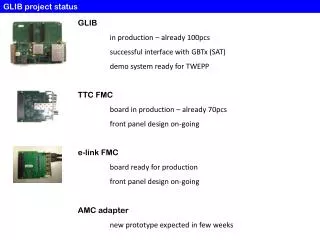
SUMMARY & OUTLOOK • 2pcs of GLIB v1 manufactured in Q1 2011, most of functionality ok, only few issues found. • All issues understood and solved in GLIB v2. 2pcs manufactured in Q3 2011. No issues found yet. • Preproduction of another 4pcs of GLIB v2 ongoing. Delivery to beta users in Mid November 2011 • FPGA with higher speed grade will be used (for 6.5Gbps transceivers) • Associated firmware, software and TTC FMC mezzanines will also be delivered. • Production version expected to be available by July 2012. • Need to define the quantity to order. If interested, please contact us by April 2012. • xTCA firmware development will start in January 2012 (xTCA infrastructure available) • Software development ongoing • Auxiliary cards under development. • TTC FMC prototype already available (2pcs + 2pcs by mid November 2011) • Versatile Link FMC, PCI Express adapter, Digital IO FMC prototypes available by Q1 2012
LINKS GLIB website GLIB Specifications document GLIB schematics GLIB at Open Hardware Repository Contact