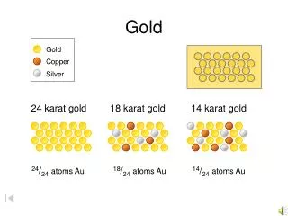
GOLD
GOLD. Generic Opto Link Demonstrator. GOLD concept. Generic demonstrator for optical input / optical output data processors Functional demonstrator for phase-0 topology processor Technology demonstrator for technologies to be used throughout L1Calo upgrade -----> ATCA form factor


GOLD
E N D
Presentation Transcript
GOLD Generic Opto Link Demonstrator
GOLD concept • Generic demonstrator for optical input / optical output data processors • Functional demonstrator for phase-0 topology processor • Technology demonstrator for technologies to be used throughout L1Calo upgrade -----> • ATCA form factor • Modular concept • Mezzanines • FMC connectors • Optical backplane connectors rather than front panel I/O • Opto/electrical conversion on input mezzanine • Electrical connectivity up to 10Gb/s in ATCA zone 2 • Phase-0 topo-specific connectivity mainly via clock mezzanine
GOLD within TP context... Add a topological processor and increase real time data path bandwidth Increase backplane bandwidth from 40Mb/s to 160Mb/s (only modifying FPGA code) GOLD Replace the merger modules Include Muon processing capability on topological processor • Backward compatible to current scheme (for staged installation)
GOLD floor plan A-J FPGAs A C front panel connectors Z3 Z3: opto connectors Mezzanines V E W B D Z2 V – Y : FMC connectors F X Z2: electrical connectors Y G H J Z1
GOLD use cases (from requirements doc.) • Demonstrator for AdvancedTCA module concept • Module form factor • Power supply concept • IPMB monitoring and control • Module control via serial protocol • Backplane transmission at 10Gb/s • Rear transition module concept • Demonstrator for Virtex-6 technologies • Demonstrator for optical backplane connection • Test bench for topological algorithms • Test bench for future LHC clock distribution schemes • Optical data sink for L1Calo modules • Optical data source for purpose of self-test and stand-alone link tests • Electrical data source/sink for tests with various electronics modules (limited bandwidth only)
Some details Main board, ATCA sized, 22 PCB layers • FPGAs • Main power distribution network (central and POL regulators) • Connectors, including e/o converters for RTDP output and non-RTDP connectivity • FPGA configurator circuitry • Some local crystal clocks (for DAQ/ROI, Ethernet, configurator) Input mezzanine module • Moderate PCB cost (12 layers, moderate real estate) • Sockets, secondary power distribution, some CPLD-based control, 10Gb/s fanout • Use daughter PCB routing rather than X-bar switches to adapt to GOLD use cases • Allow for migration to higher density o/e converter modules, should they appear on the market.
Some more details… Clock mezzanine module • Recover and condition incoming (LHC bunch) clocks • Generate local crystal clock • Some limited multiplexing and fan-out • RTDP clocks 40.08MHz and multiples only • Allow for some real estate for general control circuitry (that’s not yet defined at this stage) • Allow for flexible use of scarce low-latency off-board differential electrical connectivity USB/JTAG mezzanine • Initial scheme to provide minimum communication before FPGAs are configured • Use for Xilinx/Impact and Chipscope access during initial module tests
GOLD acting as a topo demonstrator Initial board setup with LX240 devices only: • Two-stage processing in four input processors and a main processor • Real-time input into GOLD main board: 96 links (24 per input processor), 6.4Gb/s line rate • Input mezzanine real estate for 12*12-way receivers • Backplane optical connectivity 5 sockets * 12/24/… fibres • Electrical real-time output, up to 12 LVDS pairs via clock mezzanine, to front panel • LHC bunch clock and L1A via clock mezzanine module carrying either a TTCdec or GBT circuitry (two distinct module versions) • One SFP module each for DAQ and ROI data. Input section of the SFPs available for purpose of optically distributed clock signal • Module control via serialised VME-- , or via Ethernet (Phy on clock mezzanine) • Environmental monitoring via I2C (IPMB) • FPGA configuration via SystemACE
Signal integrity – 10Gb/s • No PCB simulation tools available right now • BLT module has been designed without simulation and happens to work up to 6.4 Gb/s electro/optical data transmission • Design 10Gb/s tracks with small numbers of vias, top to bottom layer only, to avoid stubs. • Keep in-pair skew on 10Gb/s links below 5ps • PCB manufacturer in charge of differential track impedance control (100R +/- 10%) • Impedance of via pairs unknown, expect some discontinuity there. Via drill diameter and distance dictated by PCB mechanics (aspect ratio etc.) and therefore not subject to impedance control
GOLD floor plan • Z3 • 5 * XC6VLX (Processor L, main processorM) up to 36 links each • Two pairs of XC6VHX (H) 72 links each • 5+ 12-channel optos on daughter • Clock generation • 144 multigigabit input links in zone 2 (equiv. 22300 bit / BC) • L • L • Opto • M • L • L • H • H • Z2 • 890Gb/s • total • H • H • Z1
Some GOLD history • Module originally planned for 5 - 9 devices 6VLX550T, with opto backplane connection only, SNAP12 based • Converted to a mixed scheme 6VLXT / 6VHXT (6.5/10Gbps) • Added electrical backplane connectivity in ATCA Zone 2 • Learned about power consumption of Virtex 6 re-design of on-module power distribution • Ran into problems with differential auto routing / automated pin swaps • Decided to hand route it all ! • Over months increased GOLD PCB layer count from 16 to 22 to fit all tracks • Converted o/e transceivers from SNAP12 to Avago style footprint • Modified power distribution for MGT supplies again due to new assessment (XPower) of probable dissipation
Deliverables • Minimum of two GOLD PCBs • Initial module assembled with small number of FPGAs only (two?) • Incremental assembly • If incremental assembly turns out to be difficult, but GOLD proves operational so far, assemble 2nd copy with larger number of devices • Currently total of 5 LXT devices waiting on the shelves, any further quantities would need to be purchased. • Planning for several iterations of clock mezzanine and input mezzanine modules. Quantities tbd. • Current input mezzanine is meant to be a standalone test adapter with four 12-channel receivers and two 12-channel transmitters • Some initial board service firmware and software will be available soon • Algorithmic firmware under way
Plans • Some final cleanup on the design (couple of weeks) • PCB production (28 days, ie. ~6 weeks !) • Assembly (?) • On-going development of • Service firmware • Algorithmic firmware • Online software (non-GUI, non-HDMC)