http:// www.nano.anl.gov
210 likes | 421 Vues
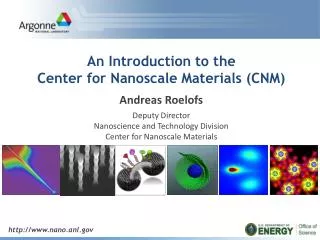
An Introduction to the Center for Nanoscale Materials (CNM). Andreas Roelofs Deputy Director Nanoscience and Technology Division Center for Nanoscale Materials. http:// www.nano.anl.gov. Center for Nanoscale Materials.

http:// www.nano.anl.gov
E N D
Presentation Transcript
An Introduction to theCenter for Nanoscale Materials (CNM) Andreas Roelofs Deputy DirectorNanoscience and Technology DivisionCenter for Nanoscale Materials http://www.nano.anl.gov
Center for Nanoscale Materials National user facility providing expertise, instruments and infrastructure for nanoscience and nanotechnology • Cross-cutting facilities: • Computational nanoscience • Dedicated hard X-ray nanoprobe at the APS • Materials synthesis and assembly • Nanofabrication research • Proximal probes • ~ 60 Staff, 20-30 Postdocs • Supports basic and applied research as well as the development of advanced instrumentation to generate new scientific insights and create innovative materials with novel properties • Academic, industrial, and international researchers have access via peer-reviewed proposals • Strong internal science program (50% own research, 50% supporting users) …has to be Nanoscience
An Integrated Vision for the CNM Nanofabrication of novel architectures Materials design and discovery CNM a scientific user facility to create, explore and control the nanoworld Simulations of the nanoworld Imaging and visualization at the nanoscale
Six integrated research groups Electronic & Magnetic Materials and Devices (EMMD) Nanobio Interfaces (NBI) CNM Facility Theory and Modeling (TMG) Nanofabrication and Devices (NFD) X-ray Microscopy (XMG) Nanophotonics (NPG)
CNM Facilities and Capabilities • ~13,000 sq. ft. of conventional research laboratories • Chemical labs • Characterization instruments • Laser-controlled area (LCA) • ~11,500 sq. ft. of cleanroom laboratories and support areas • ~6000 sq. ft. high-bay facility for scanning probe microscopes • 4are under construction • Also contains an LCA • High-Performance Computing Cluster Carbon(3000 cores, 25 TeraFLOPS) • Hard X-ray Nanoprobe – beam-line attached to the APS and co-managed • Received R&D100 award in 2009
CNM’s User Community • Access is free for non-proprietary work, including for industrial users • Users from 38 states plus Puerto Rico, in addition to a further 20 countries Recent Industrial Users Hewlett-Packard IBM Toyota Seagate AKHAN Technologies Advanced Diamond Tech. BAE Systems GE
Attracting Industrial Users • Leverage our Staff to reach out to industry • explain benefits of increasing the interaction with industry (diversity, great research done at industry – let’s participate!) • how/where to find and engage with industry (conferences, papers, notice industry affiliations) • target “5-10 years out” industry projects • Website for industrial users (at CNM and ANL website) • Held workshop targeted at industrial users in May 2013 • Established one collaborative research and development agreement • 2 licenses to CNM Staff patents granted CNM website:
CNM Staff Highlight Sequential Infiltration Synthesis (SIS)US Patent App 13209190 US Provisional Patent App • SIS-enhancement of resists for e-beam lithography, photolithography, and block copolymer lithography will enable simple fabrication of high-aspect-ratio nanostructures 100 nm Seth Darling Jeff Elam (ES) 100 nm SIS is a process by which inorganic materials can be grown within polymer films and where the reactions can be selective for specific blocks within a block copolymer film
CNM User Highlight: Mapping of Strain Fields in Semiconductor Structures using the X-ray Nanoprobe • Clarifying the spatial distribution of the strain enables optimization of strain-induced CMOS device efficiency • The Si3N4 liner transfers stress into the silicon-on-insulator (SOI) material • In situ mapping of the subsurface strain with high spatial resolution using the Hard XrayNanoprobe at CNM enabled a good model of the stress distribution to be obtained. Cross-section of a SOI/Si3N4 stressor structure C. E. Murray1, A. Ying2, S. M. Polvino2, I. C. Noyan2, M. Holt3, and J. Maser3, J. Appl. Phys.109, 083543 (2011). Measured and calculated lattice-tilt in the SOI under the Si3N4stressor. Inset: cross-sectional geometry of the sample and the direction of lattice tilt 1) IBM; 2) U Columbia; 3) CNM
Observing the nanoscale origins of memory resistive switching using the Hard X-ray Nanoprobe • Users from Hewlett-Packard Labs • High resolution x-ray fluorescence microscopy identified nanoscale metallic channel regions formed during memristive switching in a TaO metal/oxide/metal device structure Images show the presence of a Ta-rich Ta oxide phase at site of low resistance channels J. P. Strachan et al., Appl. Phys. Lett.98, 242114 (2011). 11
Nanobio Interfaces – User Science Biofunctionalized magnetic-vortex microdiscs for targeted cancer-cell destruction Univ. of Chicago Pritzker School of Medicine, Argonne Nature Materials, 2010, Kim et al. ABC News Healthbeat Segment: Shaking Up Cancer (3 min video) http://abclocal.go.com/wls/story?section=news/health&id=7245605 ac magnetic field ~10s Hz
Batteries Get a Quick Charge with New Anode Technology Catalytic Production of Clean Fuel Methane dissociation on Zn doped La2O3(001) to produce H2 without CO2 • Catalytic dissociation of methane is an environmentally friendly approach towards CO2-free production of hydrogen • First-principles computations of nanoscale surface regions show that doping oxides with low-valence atoms increases efficiency • Amorphous TiO2 nanotubes self-organize to crystalline cubic phase during Li cycling • Capacity and recharging rate greatly increased Users from U California- Santa Barbara E. W. McFarland and H. Metiu, Chem. Rev., DOI: 10.1021/cr300418s; B. Li and H. Metiu, J. Phys. Chem. C 115 (37), 18239 (2011) Users from CNM, CSE, XSD, U Chicago H. Xiong et al., J. Phys. Chem. C, 116, 3181 (2012)
Development of PlasmonicNanophotocatalysts Surface Properties of Graphene 60 nm Synthesizing graphenefor large-scale integration is a key challenge: atomic-resolution STM helps guide us towards defect-free graphene L. Gao et al., Nano Lett.10, 3512 (2010) Methylene blue dye is used as an optical probe of organic degradation AgCl:Ag hybrid nanoparticlesexhibit high efficiency and recyclability for catalysis of organic pollutant decomposition in sunlight. Graphene provides a novel support of transition metal catalyst nanoparticles Users from U Illinois Urbana-Champaign and State Key Lab on Petroleum, China C.H. An et al., Adv. Mater.22, 2570 (2010) Users from U Wisconsin-Madison E. Cho et al., J. Phys. Chem.C116, 26066 (2012)
Nanotechnology at the CNM: • Solar energy conversion • Energy storage • Catalysis • Advanced medical therapies • Information processing and storage • Sensors and electronics (detectors!) • Light emitting devices • Lithography • X-ray optical elements 90 nm 500 nm
Micro & Nanotribology Nanostructured Carbon Based Materials 3D C Diamond nanowire sensors 1D 2D Diamond micro-resonators Nanowire production from diamond template Low temp. deposition (~400C) AniSumant, Nanofabrication & Devices Group Diamond based MEMS switch CNT carbon nanotube based bio-sensors Graphene-on-diamond devices
Controlled Synthesis of Colloidal Nanoparticles Ag Ag Ag MnO2 Impact is in nanosized catalysts and photocatalysts, plasmonicnanoparticlesfor nanophotonicapplications, batteries, sensors… Yugang Sun, Nanophotonics Elena Shevchenko, Nanobio Interface Iron oxide & gold quasicrystal Xiao-Min Lin, Electronic & Magnetic Mat. and Devices
Metrics: Scientific Impact Calendar Year • 5737 citations so far for publications from CY10-CY12 • 4761 citing articles; 1363 citations for top 8 articles • IP: 71 invention reports; 36 patents filed, 10 issued 2 licensed patents
http://nano.anl.gov CNM User Access • Open submittal and review processes • public information on website • 3 calls per year • Multi-facility proposal portal • projects last for up to one year • Access is free for non-proprietary work • Flexible access modes • Proprietary & non-proprietary • Collaborative & independent • General & partner • Reviews & allocations based on feasibility & scientific merit • internal technical feasibility • external, 100+ member Proposal Evaluation Board • Notifications occur within 6-8 weeks • CNM Facility is open 40 hours/week 423 Institutions with Argonne Master User Agreements in place (as of 9/13/11) 19
CNM: a Scientific User Facility We provide State-of-the-Art capabilities and expertise 444 individual Users (2012) ~ 40 Scientific Staff Innovative staff science shapes the user program and keeps it vibrant Innovative user science helps formulate future scientific directions User facility: a unique place where many scientist gather and exchange ideas and interact
Going forward: Increase in complexity Nanotechnology by design Combining many different functionalities and different materials Add complex nanomaterials into devices Embrace non-linarites
