Introduction to Semiconductor Materials
300 likes | 319 Vues
This lecture provides an overview of semiconductor materials, including their properties and doping. It also discusses the different types of semiconductors, such as crystalline and non-crystalline, and their electronic properties. The lecture includes readings from Howe & Sodini, as well as Rabaey et al., and is available at Copy Central on Hearst Ave.

Introduction to Semiconductor Materials
E N D
Presentation Transcript
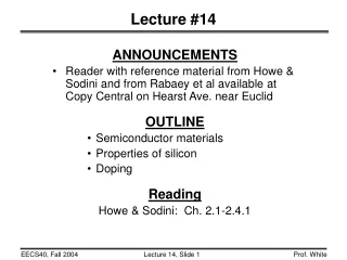
Lecture #14 ANNOUNCEMENTS • Reader with reference material from Howe & Sodini and from Rabaey et al available at Copy Central on Hearst Ave. near Euclid OUTLINE • Semiconductor materials • Properties of silicon • Doping Reading Howe & Sodini: Ch. 2.1-2.4.1
V I _ + W t homogeneous sample L (Units:W) Resistance where r is the resistivity Electrical Resistance (Units:W-cm)
Low resistivity => “conductor” High resistivity => “insulator” Intermediate resistivity => “semiconductor” Generally, the semiconductor material used in integrated-circuit devices is crystalline In recent years, however, non-crystalline semiconductors have become commercially very important What is a Semiconductor? polycrystalline amorphous crystalline
Semiconductor Materials • Elemental: • Compound:
14 electrons occupying the 1st 3 energy levels: 1s, 2s, 2p orbitals filled by 10 electrons 3s, 3p orbitals filled by 4 electrons To minimize the overall energy, the 3s and 3p orbitals hybridize to form 4 tetrahedral 3sp orbitals Each has one electron and is capable of forming a bond with a neighboring atom The Silicon Atom
Each Si atom has 4 nearest neighbors lattice constant = 5.431Å The Si Crystal “diamond cubic” lattice
Compound Semiconductors • “zinc blende” structure • III-V compound semiconductors: GaAs, GaP, GaN, etc. • important for optoelectronics and high-speed ICs
Silicon is a semiconductor material. Pure Si has relatively high resistivity at room temperature. There are 2 types of mobile charge-carriers in Si: Conduction electronsare negatively charged. Holesare positively charged. They are an “absence of electrons”. The concentration of conduction electrons & holes in a semiconductor can be affected in several ways: by adding special impurity atoms (dopants) by applying an electric field by changing the temperature by irradiation Electronic Properties of Si
Si Si Si Si Si Si Si Si Si Conduction Electrons and Holes 2-D representation When an electron breaks loose and becomes a conduction electron, a hole is also created. Note: A hole (along with its associated positive charge) is mobile!
n = number of mobile electrons per cm3 p = number of holes per cm3 ni= intrinsic carrier concentration (#/cm3) In a pure semiconductor, n = p = ni Definition of Parameters
Generation • We have seen that conduction (mobile) electrons and holes can be created in pure (intrinsic) silicon by thermal generation. • Thermal generation rate increases exponentially with temperature T • Another type of generation process which can occur is optical generation • The energy absorbed from a photon frees an electron from covalent bond • In Si, the minimum energy required is 1.1eV, which corresponds to ~1 mm wavelength (infrared region). 1 eV = energy gained by an electron falling through 1 V potential = qeV = 1.6 x 10-19 C x 1 V = 1.6 x 10⁻¹⁹ J. • Note that conduction electrons and holes are continuously generated, if T > 0
Recombination • When a conduction electron and hole meet, each one is eliminated, a process called “recombination”. The energy lost by the conduction electron (when it “falls” back into the covalent bond) can be released in two ways: • to the semiconductor lattice (vibrations) “thermal recombination” semiconductor is heated • to photon emission “optical recombination” light is emitted • Optical recombination is negligible in Si. It is significant in compound semiconductor materials, and is the basis for light-emitting diodes and laser diodes.
Generation and Recombination Rates • The generation rate is dependent on temperature T, but it is independent of n and p : • The recombination rate is proportional to both n and p: • In steady state, a balance exists between the generation and recombination rates. • A special case of the steady-state condition is thermal equilibrium: no optical or electrical sources
Pure Si conduction ni 1010 cm-3 at room temperature
Donors: P, As, Sb Acceptors: B, Al, Ga, In Doping By substituting a Si atom with a special impurity atom (Column V or Column III element), a conduction electron or hole is created. Dopant concentrations typically range from 1014 cm-3 to 1020 cm-3
Charge-Carrier Concentrations ND: ionized donor concentration (cm-3) NA: ionized acceptor concentration (cm-3) Charge neutrality condition: ND + p = NA + n At thermal equilibrium, np = ni2 (“Law of Mass Action”) Note: Carrier concentrations depend on net dopant concentration (ND - NA) !
and and N-type and P-type Material If ND >> NA(so that ND – NA >> ni): n >> p material is “n-type” If NA >> ND(so that NA – ND >> ni): p >> n material is “p-type”
Terminology intrinsic semiconductor: “undoped” semiconductor electrical properties are native to the material extrinsic semiconductor: doped semiconductor electrical properties are controlled by the added impurity atoms donor: impurity atom that increases the electron concentration group V elements (P, As) acceptor: impurity atom that increases the hole concentration group III elements (B, In) n-type material: semiconductor containing more electrons than holes p-type material: semiconductor containing more holes than electrons majority carrier: the most abundant carrier in a semiconductor sample minority carrier: the least abundant carrier in a semiconductor sample
2 3 1 electron 4 5 Carrier Scattering • Mobile electrons and atoms in the Si lattice are always in random thermal motion. • Average velocity of thermal motion for electrons in Si: ~107 cm/s @ 300K • Electrons make frequent “collisions” with the vibrating atoms • “lattice scattering” or “phonon scattering” • Other scattering mechanisms: • deflection by ionized impurity atoms • deflection due to Coulombic force between carriers • The average current in any direction is zero, if no electric field is applied.
2 3 1 electron 4 5 E Carrier Drift • When an electric field (e.g., due to an externally applied voltage) is applied to a semiconductor, mobile charge-carriers will be accelerated by the electrostatic force. This force superimposes on the random motion of electrons: • Electrons drift in the direction opposite to the E-field Current flows • Because of scattering, electrons in a semiconductor do not achieve constant acceleration. However, they can be viewed as classical particles moving at a constant average drift velocity.
n p Drift Velocity and Carrier Mobility Mobile charge-carrier drift velocity is proportional to applied E-field: | v | = mE m is the mobility (Units: cm2/V•s) Note: Carrier mobility depends on total dopant concentration (ND + NA) !
+ + + Current Density The current density J is the current per unit area (J = I/ A ; A is the cross-sectional area of the conductor) If we have N positive charges per unit volume moving with average speed v in the +x direction, then the current density in the +x direction is just J = qNv Example: 2 x10¹⁶ holes/cm3 moving to the right at 2 x104 cm/sec J = 1.6x10-19 x2x1016 x 2x104 = 64 A/cm2 v Suppose this occurs in a conductor 2 mm wide and 1 mm thick: I = J x A = 64 x (2x10-4 x1x10-4) = 1.28 mA
electron current density: hole current density: Electrical Conductivity s When an electric field is applied, current flows due to drift of mobile electrons and holes: total current density: conductivity (Units: W-cm-1)
for n-type mat’l for p-type mat’l Electrical Resistivity r (Units: ohm-cm)
From mvs. ( NA + ND ) plot Example Consider a Si sample doped with 1016/cm3 Boron. What is its resistivity? Answer: NA = 1016/cm3 , ND= 0 (NA >> ND p-type) p 1016/cm3 and n 104/cm3
Example (cont’d) Consider the same Si sample, doped additionally with 1017/cm3 Arsenic. What is its resistivity? Answer: NA = 1016/cm3, ND= 1017/cm3 (ND>>NA n-type) n 9x10¹⁶/cm3 and p 1.1x10³/cm3 The sample is converted to n-type material by adding more donors than acceptors, and is said to be “compensated”.
Sheet Resistance Rs (Unit: ohms/square) Rs is the resistance when W = L (L, W, t = length, width, thickness) • The Rs value for a given layer in an IC technology is used • for design and layout of resistors • for estimating values of parasitic resistance in a circuit R = Rs R = Rs/2 R = 2Rs R = 3Rs R 2.6Rs Metallic contacts
Integrated-Circuit Resistors The resistivity and thickness t are fixed for each layer in a given manufacturing process t A circuit designer specifies the length L and width W, to achieve a desired resistance R fixed designable Example: Suppose we want to design a 5 kW resistor using a layer of material with Rs = 200 W/ Space-efficient layout Resistor layout (top view)
Crystalline Si: 4 valence electrons per atom diamond lattice: each atom has 4 nearest neighbors 5 x 10²² atoms/cm3 In a pure Si crystal, conduction electrons and holes are formed in pairs. Holes can be considered as positively charged mobile particles which exist inside a semiconductor. Both holes and electrons can conduct current. Dopants in Si: Reside on lattice sites (substituting for Si) Group V elements contribute conduction electrons, and are called donors Group III elements contribute holes, and are called acceptors Summary
