Download
1 / 33
330 likes | 351 Vues
L7 Lasers UConn ECE 4211 02/27/2017 F. Jain. Various laser structures: DBR-Cavity, VCSEL, DFB lasers (slides 2-4) General condition of lasing (Slide 5) Cavity lasing conditions (slide 6-8), Cavity modes (slides 9-10) Semiconductor lasers (slide 11-13) and threshed current density (14-18)

E N D
L7 Lasers UConn ECE 4211 02/27/2017 F. Jain • Various laser structures: DBR-Cavity, VCSEL, DFB lasers (slides 2-4) • General condition of lasing (Slide 5) • Cavity lasing conditions (slide 6-8), Cavity modes (slides 9-10) • Semiconductor lasers (slide 11-13) and threshed current density (14-18) • Laser characteristics Optical Power-Current Behavior (slide 19-21) • Double Heterostructure Lasers-Single mode lasers (slides 22, 23) • Laser Design Exercise (slides 24-33) Operating parameters of a laser: Cavity or Distributed Feedback type (mode separation) Edge emitting or surface emitting. Temperature sensitivity: Determines Quantum well or Wire of quantum dot laser Operating wavelength: green, red, blue, fiber optic wavelength 1.55 microns Optical power output, expected external and wall conversion efficiency, Single mode or multi-mode Threshold current density JTH Temporal and spatial coherence
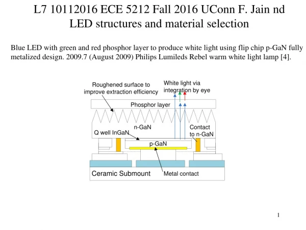
Various laser structures Fig .48 Distributed feedback (DFB) edge-emitting laser (first order grating). Fig .28. An edge-emitting cavity laser with ridge. Fig. 55 Cavity formed by one conventional mirror and one distributed Bragg reflector (DBR). Fig. 56 In a vertical cavity surface emitting laser (VCSEL) the cavity thickness is multiple of half wavelength.
W 50Ao 50Ao 50Ao p-InGaAs 1.35 mm cladding p-ZnSeTe 150 Ao B 50Ao D 100Ao B 50Ao D 100Ao B 50Ao D 150 Ao B d =(50x3)+(100x2)+(150x2)=650Aº =0.065mm 1.35 mm cladding n-ZnSeTe n-InP substrate Quantum Dot Structure Fig. 44 Active layer thickness: d = (50x3) + (100x2)+(150x2) =650Aº=0.065mm. D for dot and B for barrier.
VCSELs (vertical cavity surface emitting lasers) Fig . 58 Surface-emitting laser [Ref. J. Jahns et al, Applied Optics, 31, pp. 592-596, 1992]. Fig . 57 Photograph of a 850nm GaAs VCSEL.
General Conditions of Lasing: Rate of emission = Rate of absorption Rate of spontaneous emission + rate of stimulated emission =Rate of absorption A21N2 + B21 r(hn12) N2 = B12 r(hn12) N1 (1) Rate of stimulated emission >> rate of absorption gives B21 r(hn12) N2 >> B12 r(hn12) N1 Or, ( N2 /N1) >> 1 ………Condition known as population inversion. (Using Planck’s distribution law, we can show that B12=B21). (2) Rate of stimulated emission >> rate of spontaneous emission gives B21 r(hn12) N2 >> A21N2 Or, r(hn12) >> A21/B21 Photon density higher than a value.
Resonant Cavity: Condition I for Lasing • Gain coefficient relation with loss coefficient and losses due to light out put from mirros. • (b) Phase condition
Modes of Resonant Cavity: Figure2. Cavity with parallel end faces
Emission spectrum high lighting cavity modesFig. 3, p. 343 Figure3 shows the emission spectrum highlighting cavity modes (also known as the longitudinal or axial modes) for the GaAs laser diode. Conditions and Calculations: GaAs λ = 0.85μm nr = 3.59 L = 1000μm Δλ=2.01 Å
Population inversion in semiconductor lasers: Condition II for Lasing This condition is based on the fact that the rate of stimulated emission has to be greater than the rate of absorption. (23) Strictly speaking, the rate of stimulated emission is proportional to: (i) the probability per unit time that a stimulated transition takes place (B21) (ii) probability that the upper level E2 or Ec in the conduction band is occupied (27) , Efn = quasi-fermi level for electrons. (24) (iii) joint density of states Nj(E=hv12) (iv) density of photons with energy hv12, ρ(hv12) (v) probability that a level E1 or Ev in the valence band is empty (i.e. a hole is there) (25) The rate of stimulated emission: (26) Similarly, the rate of absorption: (27)
Using the condition that the rate of stimulated emission > rate of absorption; (assuming B21=B12), simplifying Equation (26) and Equation (27) (28) Further mathematical simplification yields if we use (29) (30) Bernard - Douraffourg Condition[1] (31) Equation (31) is the equivalent of population inversion in a semiconductor laser. For band to band transitions (32) [1]M.G.A. Bernard and G.Duraffourg, Physica Status Solidi, vol. 1, pp.699-703, July 1961
Definition of quasi Fermi-levels Gain coefficient g and Threshold Current Density Jth The gain coefficient g is a function of operating current density and the operating wavelength λ. It can be expressed in terms of absorption coefficient α(hv12) involving, for example, band-to-band transition.
Derivation of threshold current density JTH Rate of stimulated emission = B21feNj(E=h) (h12) fh (Where (h12) = P v hs) = B21fefh (vg) nNs Rate of absorption = (1-fh)(1-fe) vg nNs B12 Net rate = Stimulated – absorption = [fe fh – (1-fe)(1-fh)] vg nNs B21 = -[1-fe-fh] vg nNs B21 and also note that B12 = B21) The gain coefficient is Rate of spontaneous emission (34)
where: αovg = probability of absorbing a photon Nv = number of modes for photon per unit frequency interval Δvs = width of the spontaneous emission line Equation (34) gives (35) The total rate of spontaneous emission (36) (37) where: Rc = Rate per unit volume η = quantum efficiency of photon (spontaneous) emission d = active layer width A = junction cross-section Equations (33), (35), (36) and (37) give (38)
(39) (40) Substituting for Nv and , we get (41) The condition of oscillation, Equation (15), gives (15)
Threshold current density Using Equation (15) and Equation (42) (43) (44) • When the emitted stimulated emission is not confined in the active layer thickness d, • Γ, confinement factor is fraction of laser power in the active layer d divided by total power generated. • z(T) depends on quasi Fermi levels which depend on electron and hole concentration sin active layer. • R1 and R2 are the reflectivity . (If you cannot find them, use R1=R2=0.3) • is the quantum efficiency of photon production when electron and hole recombine. • is the absorption coefficient of light in the laser active layer. It is given. • Spontaneous line from active layer is
Laser Characteristics 5.4.1 Optical power-current characteristics: page 354 The laser diode emits spontaneously until the threshold current is exceeded (i.e. I > Ith Fig. 9). Fig. 9 Power output versus current (P-I) characteristic. Note that Pout is significant above I increments above Ith. Fig. 10 shows the V-I characteristic. Fig. 10. V-I characteristics of a laser diode.
Fig. 13. Far-field pattern of a AlGaAs-GaSs laser. Fig. 14 (a) Beam divergence in transverse/perpendicular and (b) lateral directions.
Single mode laser What would you do to obtain single transverse mode and single lateral mode operation? Select d and W for single transverse mode and lateral mode, respectively. HINT: Active layer thickness d to yield single transverse mode d < m l/[2(nr2-nr12)1/2], m=1, 2, 3, Top contact (stripe) width W for single mode:[W < m l/[2(nr,center2-nr,corner 2)1/2], m=1, 2; if you cannot find it use W=5 m]; Use nr,center –nr, corner ~0.005 in gain guided lasers. Cavity length L=500 micron to star twith (You select L such that it will result in the desired JTH and optical power output).
a. Outline all the design steps b. Show device dimensions (active layer thickness d, cavity length L and width W), doping levels of various layers constituting the laser diode (shown below in Fig. 1). 5.62 page 370--Design of an InGaAs-GaAs 980nm Laser-Level 2