Download
1 / 62
620 likes | 646 Vues
L9B Lasers ENGR_ ECE 4243_6243 UConn F. Jain 10252016. Conditions of Lasing Threshold Current Density J th Reduction of J th : Heterostructure Lasers Optical Power-Current Behavior Carrier confinement in a double Heterostructure (DH) laser Laser Design Exercise

E N D
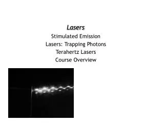
L9B Lasers ENGR_ECE 4243_6243 UConn F. Jain 10252016 • Conditions of Lasing • Threshold Current Density Jth • Reduction of Jth: Heterostructure Lasers • Optical Power-Current Behavior • Carrier confinement in a double Heterostructure (DH) laser • Laser Design Exercise • Quantum Well/Wire/dot Lasers • Distributed Feedback Lasers Operating parameters: Operating wavelength: green, red, blue, fiber optic wavelength 1.55 microns Optical power output, expected external and wall conversion efficiency, Operating structure Cavity or Distributed Feedback type Edge emitting or surface emitting.
Various laser structures Fig .48 Distributed feedback (DFB) edge-emitting laser (first order grating). Fig .28. An edge-emitting cavity laser with ridge. Fig. 55 Cavity formed by one conventional mirror and one distributed Bragg reflector (DBR). Fig. 56 In a vertical cavity surface emitting laser (VCSEL) the cavity thickness is multiple of half
W 50Ao 50Ao 50Ao p-InGaAs 1.35 mm cladding p-ZnSeTe 150 Ao B 50Ao D 100Ao B 50Ao D 100Ao B 50Ao D 150 Ao B d =(50x3)+(100x2)+(150x2)=650Aº =0.065mm 1.35 mm cladding n-ZnSeTe n-InP substrate Quantum Dot Structure Fig. 44 Active layer thickness: d = (50x3) + (100x2)+(150x2) =650Aº=0.065mm. D for dot and B for barrier.
VCSELs (vertical cavity surface emitting lasers) Fig . 58 Surface-emitting laser [Ref. J. Jahns et al, Applied Optics, 31, pp. 592-596, 1992]. Fig . 57 Photograph of a 850nm GaAs VCSEL.
General Conditions of Lasing: Rate of emission = Rate of absorption Rate of spontaneous emission + rate of stimulated emission =Rate of absorption A21N2 + B21 r(hn12) N2 = B12 r(hn12) N1 (1) Rate of stimulated emission >> rate of absorption gives B21 r(hn12) N2 >> B12 r(hn12) N1 Or, ( N2 /N1) >> 1 ………Condition known as population inversion. (Using Planck’s distribution law, we can show that B12=B21). (2) Rate of stimulated emission >> rate of spontaneous emission gives B21 r(hn12) N2 >> A21N2 Or, r(hn12) >> A21/B21 Photon density higher than a value.
General Conditions of Lasing: • Representing the amplitude/magnitude • (b) Phase condition
Resonant Cavity: Condition I for Lasing Figure2. Cavity with parallel end faces
The emission spectrum high lighting cavity modes Figure3 shows the emission spectrum highlighting cavity modes (also known as the longitudinal or axial modes) for the GaAs laser diode. Conditions and Calculations: GaAs λ = 0.85μm nr = 3.59 L = 1000μm Δλ=2.01 Å
Equivalent of population inversion in semiconductor lasers: Condition II for Lasing This condition is based on the fact that the rate of stimulated emission has to be greater than the rate of absorption. (23) Strictly speaking, the rate of stimulated emission is proportional to: (i) the probability per unit time that a stimulated transition takes place (B21) (ii) probability that the upper level E2 or Ec in the conduction band is occupied (27) , Efn = quasi-fermi level for electrons. (24) (iii) joint density of states Nj(E=hv12) (iv) density of photons with energy hv12, ρ(hv12) (v) probability that a level E1 or Ev in the valence band is empty (i.e. a hole is there) (25) The rate of stimulated emission: (26) Similarly, the rate of absorption: (27)
[1]M.G.A. Bernard and G.Duraffourg, Physica Status Solidi, vol. 1, pp.699-703, July 1961 Using the condition that the rate of stimulated emission > rate of absorption; (assuming B21=B12), simplifying Equation (26) and Equation (27) (28) Further mathematical simplification yields if we use (29) (30) Bernard - Douraffourg Condition[1] (31) Equation (31) is the equivalent of population inversion in a semiconductor laser. For band to band transitions (32)
Definition of quasi Fermi-levels Gain coefficient g and Threshold Current Density Jth The gain coefficient g is a function of operating current density and the operating wavelength λ. It can be expressed in terms of absorption coefficient α(hv12) involving, for example, band-to-band transition.
Derivation of JTH Rate of stimulated emission = B21feNj(E=h) (h12) fh (Where (h12) = P v hs) = B21fefh (vg) nNs Rate of absorption = (1-fh)(1-fe) vg nNs B12 Net rate = Stimulated – absorption = [fe fh – (1-fe)(1-fh)] vg nNs B21 = -[1-fe-fh] vg nNs B21 and also note that B12 = B21) The gain coefficient is Rate of spontaneous emission (34)
where: αovg = probability of absorbing a photon Nv = number of modes for photon per unit frequency interval Δvs = width of the spontaneous emission line Equation (34) gives (35) The total rate of spontaneous emission (36) (37) where: Rc = Rate per unit volume η = quantum efficiency of photon (spontaneous) emission d = active layer width A = junction cross-section Equations (33), (35), (36) and (37) give (38)
(39) (40) Substituting for Nv and , we get (41) The condition of oscillation, Equation (15), gives (15)
Threshold current density Using Equation (15) and Equation (42) (43) (44) When the emitted stimulated emission is not confined in the active layer thickness d, Equation (44) gets modified by Γ, the confinement factor (which goes in the denominator).
Threshold current density Using Equation (15) and Equation (42) (43) (44) • When the emitted stimulated emission is not confined in the active layer thickness d, • Γ, confinement factor is fraction of laser power in the active layer d divided by total power generated. • z(T) depends on quasi Fermi levels which depend on electron and hole concentration sin active layer. • R1 and R2 are the reflectivity . (If you cannot find them, use R1=R2=0.3) • is the quantum efficiency of photon production when electron and hole recombine. • is the absorption coefficient of light in the laser active layer. It is given. • Spontaneous line from active layer is
Laser Characteristics 5.4.1 Optical power-current characteristics: page 354 The laser diode emits spontaneously until the threshold current is exceeded (i.e. I > Ith Fig. 9). Fig. 9 Power output versus current (P-I) characteristic. Note that Pout is significant above I increments above Ith. Fig. 10 shows the V-I characteristic. Fig. 10. V-I characteristics of a laser diode.
Fig. 13. Far-field pattern of a AlGaAs-GaSs laser. Fig. 14 (a) Beam divergence in transverse/perpendicular and (b) lateral directions.
Single mode laser What would you do to obtain single transverse mode and single lateral mode operation? Select d and W for single transverse mode and lateral mode, respectively. HINT: Active layer thickness d to yield single transverse mode d < m l/[2(nr2-nr12)1/2], m=1, 2, 3, Top contact (stripe) width W for single mode:[W < m l/[2(nr,center2-nr,corner 2)1/2], m=1, 2; if you cannot find it use W=5 m]; Use nr,center –nr, corner ~0.005 in gain guided lasers. Cavity length L=500 micron to star twith (You select L such that it will result in the desired JTH and optical power output).
a. Outline all the design steps b. Show device dimensions (active layer thickness d, cavity length L and width W), doping levels of various layers constituting the laser diode (shown below in Fig. 1). --Design of an InGaAs-GaAs 980nm Laser-Level 2
AlxGa1-xAs AlxGa1-xAs GaAs V(z) ∆EC ∆Ec = 0.6∆Eg ∆Ev = 0.4∆Eg 0 z 0 ∆EV -EG z ∆EV -EG+∆EV 2.9.8 Double heterojunction with a quantum wells By reducing the thickness of p-GaAs layer to 50-100Å, we obtain a quantum well double heterostructure as shown schematically in Fig. 42B, page 173. Fig. 42 B GaAs quantum well with finite barriers produced by AlGaAs layers.
W 50Ao 50Ao 50Ao P+-InGaAs 1.35 mm cladding p-ZnSeTe 150 Ao B 50Ao D 100Ao B 50Ao D 100Ao B 50Ao D 150 Ao B d=(50x3)+(100x2)+(150x2)=650Aº=0.065mm Design a 1.3micron single mode quantum dot laser emitting 1mW. [a) Find composition of dot, barrier layers, and cladding layer. b) Find the index of refraction of active layer (find dot and barrier index and take average). c) Showd=0.065μm meets the requirement for single transverse mode. Find new W for single lateral mode. 1.35 mm cladding N+-ZnSeTe n+-InP substrate Double heterojunction with a quantum dot active layer
Heterojunctions (Band Diagram, Carrier Confinement) Heterojunctions: Single and double heterojunctions 2.9.5. Single heterojunctions: Energy band diagrams for N-AlGaAs – p-GaAs and P-AlGaAs/n-GaAs heterojunctions under equilibrium Fig. 35. Energy band diagram per above calculations. N-p heterojunction. Fig. 36. Energy band diagram for a p-n heterojunction.
Energy band diagram:Double Heterojunction Fig. 39. A forward biased NAlGaAs-pGaAs-P-AlGaAs double heterojunction diode. Fig. 42 Energy band diagram of a NAlGaAs-pGaAs-PAlGaAs double heterostructure diode.
Built-in Voltage in Heterojunctions Fig. 33. Energy band diagram line up before equilibrium.
2.9.4. Forward-Biased NAlGaAs-pGaAs Heterojunction Fig.34 Carrier concentrations in an n-p heterojunction Electron diffusion from N-AlGaAs to the p-GaAs side, Hole diffusion from pGaAs to the N-AlGaAs, (73) (162) (161) (164)
I-V Equation (170)
I-V Equation and Current Density Plot Here, we have used the energy gap difference DEg=Eg2-Eg1. From Eq. 174 we can see that the second term, representing hole current density Jp which is injected from p-GaAs side into N-AlGaAs, and it is quite small as it has [exp-(DEg/kT)] term. As a result, J ~ Jn(xp), and it is Fig. 38B Current density plots.
Carrier Confinement in lower energy gap layer in double heterojunctions Fig .41. Minority carrier concentrations in p-GaAs and in p-AlGaAs. Thus, the addition of P-AlGaAs at x=xp+d forces the injected electron concentration quite small. That is, it forces all injected carrier to recombine in the active layer. This is known as carrier confinement.
Photon confinement in lower energy gap layer in double heterojunctions Photon confinement in higher index of refraction layer (lower energy gap layer) forming a waveguide region between two wider energy gap and lower index layers (p.170) When electron and holes recombine in the GaAs layer, they produce photons. AlGaAs layers have lower index of refraction than GaAs layer. As a result it forms a natural waveguide. In the laser design example, we have mentioned various methods for the calculation of modes in such a slab waveguide. Also we need to calculate the confinement factor G of the mode. Confinement factor also determines the JTH. Generally, the confinement factor becomes smaller as the thickness of the active layer becomes narrower. This also depends on the index of refraction difference between the active and the cladding layers.
2.5.7 Energy band diagrams under forward and reverse biasing: p-n homojunction Fig. 10 showsenergy band diagrams for equilibrium, forward bias and reverse biasing conditions. We outline steps to obtain these diagrams: Step 1. Draw a straight line and call it Fermi energy under equilibrium (dashed line). Step 2. Draw two vertical lines representing junction. Note that the equilibrium width Wo (left figure) is larger than forward bias diode (center Wf) and smaller than the reverse biased diode (Wr right). Step 3.Draw new Fermi level in the neutral p-semiconductor with respect to the n-semiconductor. There is no change in equilibrium or left figure. Under forward bias, p-region is qVf lower than the equilibrium value as shown in the center figure. In forward bias of 0.2V, p-side is positive, but the electron energy band diagram is 0.2eV below the equilibrium Fermi level. The case is opposite in the reverse bias of -0.2V. Here, p-side is Vr = -0.2V negative with respect to n-side, but the new Fermi level is 0.2eV higher than the equilibrium level. Step 4. Draw valence band and conduction band on the p-side using new Fermi level. Step 5. Join conduction bands and valence bands between the two vertical lines.
Space charge region in a p-n junction under equilibrium When p-Si and n-Si are joined, there is a transfer of electrons from n-side to p-side and holes from p-side to n-side and an equilibrium state is reached. When holes leave the p-side they leave behind negatively charged acceptors and similarly, when electrons leave n-side they leave behind positively charged donors. This establishes a space charge density is shown in Fig. 4b and 4c. This in turn establishes an electric field E. Fig. 3 (above) shows the profile of carrier concentrations in the junction region. The concentration gradient dn/dx and dp/dx and electric field oppose each other. This results in an equilibrium junction width Wo.