Download
1 / 26
260 likes | 406 Vues
Silicon Microfluidic Scintillation Detectors. 1 Physics Department , European Organization for Nuclear Research (CERN), Switzerland 2 Microsystems Laboratory , Ecole Polytechnique Fédérale de Lausanne (EPFL), Switzerland

E N D
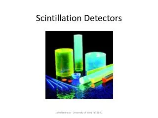
SiliconMicrofluidicScintillation Detectors 1PhysicsDepartment, European Organization for NuclearResearch (CERN), Switzerland 2MicrosystemsLaboratory, EcolePolytechniqueFédérale de Lausanne (EPFL), Switzerland 3 Sezione di Roma 1, Istituto Nazionale di Fisica Nucleare (INFN), Italy P. Maoddi1,2, A. Mapelli1, P. Bagiacchi3, B. Gorini1, M. Haguenauer1, G. Lehmann Miotto1, R. Murillo Garcia1, F. Safai Tehrani3, L. Serex1, S. Veneziano3, P. Renaud2 13th Topical Seminar on Innovative Particle and Radiation Detectors, Siena 2013
Outline • Introduction • Microfluidicscintillation detectors: concept and previous work • Advantages and applications • Single layerdevices • Fabricationtechnology • Experiments • Double layerdevices • Fabricationtechnology • Experiments • Conclusions and outlook 13th Topical Seminar on Innovative Particle and Radiation Detectors, Siena 2013
Operating Principle • Microfluidicchannelfilled with liquidscintillatordefining anarray of waveguides Microchannel Scintillation • Photodetector pixel coupledto eachchannel end • Scintillation light guidedalongmicrochannel and detected For fine spatialresolution: small channels (10 µm – 1 mm) microfluidics Photodetector array 13th Topical Seminar on Innovative Particle and Radiation Detectors, Siena 2013
First Prototype MAPMT First prototype ( first shownat IPRD08 ) • Microchannels made by SU-8 photolithography • Gold reflectivecoating DAQ system 20 mm (200 µm deepchannel) ~8 mm-1 15 mm Photo: J. Daguin A. Mapelli PhD thesis (2011) 13th Topical Seminar on Innovative Particle and Radiation Detectors, Siena 2013
Advantages And Applications Advantages • Increasedradiationresistance(liquidscintillator can be easilycirculated in microchannels) • Microfabricationtechnologyallows to makeverythin detectors Potentialapplicationsindividuated • Tracking/calorimetry in high energyphysics • Beammonitoring in hadrontherapy 13th Topical Seminar on Innovative Particle and Radiation Detectors, Siena 2013
Online BeamMonitoring • Hadrontherapy • Cancer treatment usinghadronbeams • Microfluidic detectors • Verythin detectors can be made with microfabricationtechniques • Verygoodradiationresistanceexpected Particlebeam Thinmicrofluidic detector • Real-time monitoring of the beamduringpatientirradiation • Safer treatment • Optimizedbeam time use • Treatment costreduction Patient under treatment 13th Topical Seminar on Innovative Particle and Radiation Detectors, Siena 2013
WhySilicon? SU-8 photosensitivepolymer • Easy micropatterning (one-stepphotolithography) • Goodradiationresistance (comparable to Kapton) • Mainchallenge: incompatible with high temperature processing(required for othermaterials in the device, e.g. metal bonding) Silicon • Manyreliablemicrofabricationtechniquesavailable • Betterthermal and mechanicalresistance • Possibility of tight integration of microchannels withsemiconductordevices(photodetectors, electronics, …) Allmicrofabricationactivitiesperformedat theEPFL Center for Micronanotechnologycleanroom Photo: V. Floraud 13th Topical Seminar on Innovative Particle and Radiation Detectors, Siena 2013
Dry Etching and Smoothing • RF plasma reactoralternating SF6 (etching) and C4F8 (polymercoating) plasmas • Vertical etchingprofilebutresulting in «scalloping» • Wetoxidation SiO2haslarger volume than Si surfacefeaturesloss • SiO2removal with hydrofluoric acid smoothsilicon 5 µm 2 µm 13th Topical Seminar on Innovative Particle and Radiation Detectors, Siena 2013
Dry Etching of Microchannels • Startingsubstrate: silicon wafer • Etching of microchannels via DRIE process Microchannels etched in silicon 1. Patterning of siliconoxideasetchingmask 2. DeepReactiveIonEtching(alternatedetching and passivationsteps) 3. Smoothingby thick SiO2growthand removal surfaces with suitableopticalquality 200 µm 13th Topical Seminar on Innovative Particle and Radiation Detectors, Siena 2013
Optical Coating and Bonding 0.5 mm • Deposition of reflectivealuminumlayer • Wafer-levelbonding of metallizedglass top 0.5 mm 4. Reflectivecoatingby aluminum sputtering Bondedchannelssection Twodevicessuperimposed and staggered 5. Preparation of top cover (aluminumpatterning on glass wafer) Pyrex 100 µm 6. Anodicbonding Total thickness ~0.96 mm 13th Topical Seminar on Innovative Particle and Radiation Detectors, Siena 2013
Optical and Fluidic Packaging Microchannels cut open 15 mm 7. Dicing Channel ends are cut open Finisheddevice 20 mm 8. «Packaging» Thinglasswindow and fluidicconnectorsglued on chip 13th Topical Seminar on Innovative Particle and Radiation Detectors, Siena 2013
Characterization with PMTs Event count Radioactivesource (90Sr ) (180µm deepchannel) ~7.8 mm-1 Charge signal QDC PMT Photoelectronspectrumfitted with: PMT Signal Gaussiansconvoluted with Poissondistribution (PMT response) Pedestal Scintillatingfiber(trigger) β- 13th Topical Seminar on Innovative Particle and Radiation Detectors, Siena 2013
Light Yield • Expected light yieldconsistent with PMT measurements 2.07 (measured: 1.42) PMT quantum efficiency (~0.25) Interface opticalefficiency (~0.9) Needsimprovement! Light transportefficiency (~0.03) Averagescintillationphotons (~307) 50 µm Effects of surfaceroughness and defectsat the liquid/glue/glassinterface(lowering) notcalculated! Possiblesolution: lowrefractiveindexdielectriccladding 13th Topical Seminar on Innovative Particle and Radiation Detectors, Siena 2013
BeamMonitoring • High flux of relatively high energyparticles • High light output expected • No need for high sensitivityphotodetectors Energy distribution Particlebeam x x Hamamatsu S8866-128-02 photodiode array 13th Topical Seminar on Innovative Particle and Radiation Detectors, Siena 2013
Experiments with Photodiodes Photodiode (pixel) 0.8 Integrated light signal x Plastic support 0.8 0.18 . . . Microchannels (mm) 0.7 Microchannel section Pixel number (0 … 127) β- Microchannels windowon photodiodes 90Sr source (2.4 MBq) Long integration time used (1 sec) Hamamatsu S8866-128-02photodiode array (connected to DAQ board) Readoutsystemdeveloped in collaboration with INFN Rome 13th Topical Seminar on Innovative Particle and Radiation Detectors, Siena 2013
Experiments with Photodiodes Problem: flux from radioactive source toolow for scintillationphotons to «sum-up» in the photodiodes • Test setup 90Sr source: ~104 e-/sec @ ~2 MeV/e- • For comparison,protontherapy: ~1011 p+/sec @ ~100 MeV/p+ Conclusions: • Test setup with 90Sr source notsuitable for readout with photodiodes • Test with actualbeamenvisioned to validate thiskindof application 13th Topical Seminar on Innovative Particle and Radiation Detectors, Siena 2013
Double LayerMicrochannels Patentfiled in 2012, PCT/EP2012001980 • Adding an orthogonalmicrochannellayer XY position resolution • Technologicalsolution:patterningbothsides of the siliconsubstrate y x X side Y side 13th Topical Seminar on Innovative Particle and Radiation Detectors, Siena 2013
WetEtching of XY Microchannels • Startingsubstrate: silicon wafer • Etching of microchannels on bothsidesat the same time 1. Patterning of etchingmask on bothsides of the wafer 2. Etching of bothsides of the wafer 3. Reflectivecoating by aluminum Sputtering on bothsides 13th Topical Seminar on Innovative Particle and Radiation Detectors, Siena 2013
Packaging of Double Layer Chips • One-stepbonding of 3 wafersstack • Dry etching for inter-layer connection Si Bondinginterface Al 200 nm Silicon or pyrex cover wafers Si 4. Bonding of 3 wafersstackby aluminumthermocompression Fluidinlet Top layer 5. Channel cutting and gluing of two glass windows and fluidic connectors as before 80 µm inter-layer Si Bottom layer 13th Topical Seminar on Innovative Particle and Radiation Detectors, Siena 2013
Experiments with XY devices (preliminary) X layer (150 µm) Radioactivesource (90Sr ) X PMT Y PMT Data acquisition from bothlayersat the same time Trigger PMT (preliminary) Y layer (150 µm) β- Trigger fiber ~6 mm-1 (Glass windows and tubingnotshown) 13th Topical Seminar on Innovative Particle and Radiation Detectors, Siena 2013
Conclusions and Outlook Conclusions • Differentprocesses for microchannelpatterning on silicondeveloped • Single and double layerdevicesdemonstrated with PMT readout • Issues on tests with photodiode array readout Perspectives • Beamtests with photodiodereadout • Integration of on-chip a-Si:Hphotodiodes • Readoutsystembased on SiPMs 13th Topical Seminar on Innovative Particle and Radiation Detectors, Siena 2013
Other Technologies ... aside from silicon, research on polymeric microchannelsalsoongoing! 200 µm 110 µm totalthickness(30 + 50 + 30) ~0.03% X0 20 x 20 mm 13th Topical Seminar on Innovative Particle and Radiation Detectors, Siena 2013
ThankYou 13th Topical Seminar on Innovative Particle and Radiation Detectors, Siena 2013
Staggering • Staggeredchannels for improvedgeometricalcoverage 100 µm staggering Pyrex grinded to 100 µm Total thickness ~0.96 mm (focal plane in the middle) 13th Topical Seminar on Innovative Particle and Radiation Detectors, Siena 2013
Material Budget 0.5 mm Excessmaterial can be ground down to 100 – 50 µm Single layer: 0.12% to 0.28%X0 Double layer: 0.24% to 0.5%X0 min max 13th Topical Seminar on Innovative Particle and Radiation Detectors, Siena 2013
FluidicOperation 24h operationatΔP = 1 bar:lessthan 80 mL of scintillatorneeded Channel section depth width 13th Topical Seminar on Innovative Particle and Radiation Detectors, Siena 2013