Download
1 / 66
660 likes | 844 Vues
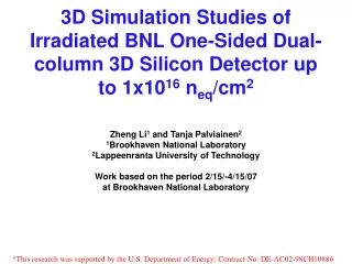
3D Simulation Studies of Irradiated BNL One-Sided Dual-column 3D Silicon Detector up to 1x10 16 n eq /cm 2. Zheng Li 1 and Tanja Palviainen 2 1 Brookhaven National Laboratory 2 Lappeenranta University of Technology Work based on the period 2/15/-4/15/07 at Brookhaven National Laboratory.

E N D
3D Simulation Studies of Irradiated BNL One-Sided Dual-column 3D Silicon Detector up to 1x10¹⁶ neq/cm2 Zheng Li1 and Tanja Palviainen2 1Brookhaven National Laboratory 2Lappeenranta University of Technology Work based on the period 2/15/-4/15/07 at Brookhaven National Laboratory *This research was supported by the U.S. Department of Energy: Contract No. DE-AC02-98CH10886
OUTLINE • Simulated detector structure • Simulation tools • Simulated full depletion voltage up to 1x10¹⁶ neq/cm2 • 3D profiles of hole concentration and E-field up to 1x10¹⁶ neq/cm2 • Various other geometries • Summary
Detector Structure • BNL’s one-sided, dual column 3D detector • There are two n-type (blue) and two p-type (red) doped columns on p-type substrate • Same type of doped columns are placed to the opposite corners n+ Front-side: processing side 270 µm p+ Backside: floating with SiO2 =50 µm p+ n+ p+ =10 µm 300 µm p, 10k-cm n+ p+ n+
Simulation • Silvaco DEVEDIT3D, DEVICE3D (ATLAS) • The detector structure was simulated with different fluencies (Neff) • Oxide charge of 4x10¹¹ /cm2 is implemented • 3D hole and E-field profiles are simulated
Simulated Vfd values in dual column 3D detectors with different fluencies Current vs. V (no lifetime degradation entered) Vfd 3D is 1.4 times higher: Small electrodes
5x10¹⁴ neq/cm2 • 200V, hole conc., electric field n+ Hole concentration n+ p+ p+ E-field p+ p+
1x10¹⁵ neq/cm2 • 200V, hole conc., electric field n+ Hole concentration n+ p+ p+ E-field p+ p+
2x10¹⁵ neq/cm2 • 200V, hole conc., electric field n+ Hole concentration n+ p+ p+ E-field p+ p+
3x10¹⁵ neq/cm2 • 200V, hole conc., electric field n+ Hole concentration n+ p+ p+ E-field p+ p+
4x10¹⁵ neq/cm2 • 200V, hole conc., electric field n+ Hole concentration n+ p+ p+ E-field p+ p+
5x10¹⁵ neq/cm2 • 200V, hole conc., electric field n+ Hole concentration n+ p+ p+ E-field p+ p+
6x10¹⁵ neq/cm2 • 200V, hole conc., electric field n+ Hole concentration n+ p+ p+ E-field p+ p+
7x10¹⁵ neq/cm2 • 200V, hole conc., electric field n+ Hole concentration n+ p+ p+ E-field p+ p+
8x10¹⁵ neq/cm2 • 200V, hole conc., electric field n+ Hole concentration n+ p+ p+ E-field p+ p+
9x10¹⁵ neq/cm2 • 200V, hole conc., electric field n+ Hole concentration n+ p+ p+ E-field p+ p+
1x10¹⁶ neq/cm2 • 200V, hole conc., electric field n+ Hole concentration n+ p+ p+ E-field p+ p+
9x10¹⁵ neq/cm2 (200V) • hole conc. p+ n+ p+ n+ Hole concentration
9x10¹⁵ neq/cm2 (200V) • hole conc. p+ n+ p+ n+ Hole concentration
9x10¹⁵ neq/cm2 (200V) • hole conc. p+ n+ p+ n+ Hole concentration
9x10¹⁵ neq/cm2 (200V) • hole conc. p+ n+ p+ n+ Hole concentration
9x10¹⁵ neq/cm2 (200V) • hole conc. p+ n+ p+ n+ Hole concentration
9x10¹⁵ neq/cm2 (200V) • hole conc. p+ n+ p+ n+ Hole concentration
9x10¹⁵ neq/cm2 (200V) • hole conc. p+ n+ p+ n+ Hole concentration
9x10¹⁵ neq/cm2 (200V) • hole conc. p+ n+ p+ n+ Hole concentration
9x10¹⁵ neq/cm2 (200V) • hole conc. p+ n+ p+ n+ Hole concentration
9x10¹⁵ neq/cm2 (200V) • hole conc. p+ n+ p+ n+ Hole concentration
9x10¹⁵ neq/cm2 (200V) p+ n+ p+ n+ Hole concentration The volume under the columns can be depleted with modest E-field: not dead area, and providing a sensitivity under the columns
9x10¹⁵ neq/cm2 (200V) • hole conc. p+ n+ p+ n+ Hole concentration
9x10¹⁵ neq/cm2 (200V) • hole conc. p+ n+ p+ n+ Hole concentration
9x10¹⁵ neq/cm2 (200V) • electric field p+ n+ p+ n+ E-field
9x10¹⁵ neq/cm2 (200V) • electric field p+ n+ p+ n+ E-field
9x10¹⁵ neq/cm2 (200V) • electric field p+ n+ p+ n+ E-field
9x10¹⁵ neq/cm2 (200V) • electric field p+ n+ p+ n+ E-field
9x10¹⁵ neq/cm2 (200V) • electric field p+ n+ p+ n+ E-field
9x10¹⁵ neq/cm2 (200V) • electric field p+ n+ p+ n+ E-field
9x10¹⁵ neq/cm2 (200V) • electric field p+ n+ p+ n+ E-field
9x10¹⁵ neq/cm2 (200V) • electric field p+ n+ p+ n+ E-field
9x10¹⁵ neq/cm2 (200V) • electric field p+ n+ p+ n+ E-field
9x10¹⁵ neq/cm2 (200V) • electric field p+ n+ p+ n+ E-field
9x10¹⁵ neq/cm2 (200V) • electric field p+ n+ p+ n+ E-field
9x10¹⁵ neq/cm2 (200V) • electric field p+ n+ p+ n+ E-field
9x10¹⁵ neq/cm2 (200V) • electric field p+ n+ p+ n+ E-field
Varieties in detector geometry • The pad size (Lc) and the distance between pads (Lp) were varied Lp Lc Lc
Lc=3um, Lp=10um • 200V, hole conc., electric field n+ Hole concentration n+ E-field p+ p+ p+ p+
Lc=3um, Lp=20um • 200V, hole conc., electric field n+ Hole concentration n+ E-field p+ p+ p+ p+
Lc=5um, Lp=30um • 200V, hole conc., electric field n+ Hole concentration n+ E-field p+ p+ p+ p+
Lc=5um, Lp=40um • 200V, hole conc., electric field n+ Hole concentration n+ E-field p+ p+ p+ p+
Lc=5um, Lp=50um • 200V, hole conc., electric field n+ Hole concentration p+ n+ p+ E-field p+ p+
Simulated Vfd values for different geometries in detector Lp≤ 30um With lifetime degradation
BNL-2C-3D, p-type bulk (300 µm), p+ and n+ columns (270 µm) LP = 30 µm, 1x10¹⁶ neq/cm2, V = 150 V Front side p+ n+ n+ p+ Full 3D detectors with reduced column spacing LP LP~ dCCE --- less trapping Smaller V --- no breakdown problem Backside