Download
1 / 23
230 likes | 586 Vues
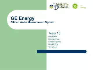
GE Energy Silicon Wafer Measurement System. Team 10 Olin Biddy Scott Johnson Chetwyn Jones Rob McCoy Tim Weber. Project Overview. Design a device that can measure the thickness of a silicon wafer Silicon wafer production has to be precise Wafers come off a conveyer belt from oven

E N D
GE Energy Silicon Wafer Measurement System Team 10 Olin Biddy Scott Johnson Chetwyn Jones Rob McCoy Tim Weber
Project Overview • Design a device that can measure the thickness of a silicon wafer • Silicon wafer production has to be precise • Wafers come off a conveyer belt from oven • Immediate feedback for production adjustments • Important Requirements • Accurate within 10 microns • 9 or more measurement points • Completes process in 30 seconds • Repeatable and Reproducible
Goals of Prototype • Detects faulty wafers • Outputs thickness measurements in user friendly format • Store data for further research / analysis • Easy to operate for workstation user • Graphical representation of surface geometry
Design Requirements: Wants Precision- Degree to which future measurements will show similar results. Accuracy- Degree of conformity of measured value to its true value.
Design Requirements: Metrics Prioritized List of Metrics Gage Reproducibility and Repeatability – Measures Precision using Statistical Process Control equation.
Concept Selection Infrared Laser- Two laser heads fixed in place. Wafer slides between lasers on XY Table Precision Linear Gauges- Two grids of 9 linear gauges fixed, one grid on each side of wafer
Complete Concept • Two lasers for subtraction measurement method • XY Table to transverse wafer • Stage to hold wafer between laser heads • Stationary frame for laser heads • Labview to control XY Table, lasers and analyze data System Components
LK-G Laser • Accurate up to .05 microns • Fast 20,000 measurements a second • Auto-adjusts intensity for changing reflectivity • Wide Spot of 850 microns to average over pits on surface • Connectivity with Labview for data collection
XY- Table (Velmex, Inc.) • Stable movement • Stepper motor drives • 9”x9” travel of 12”x12” work surface • .001” resolution • Vmax = 4.0 in/s • LabView interface • Easy attachment for wafer stage
Wafer Stage • Two stage platforms to accommodate both 6”x6” and 9”x7” wafers • Press fit pins allow for quick change between top wafer platforms • Rubber surface to eliminate wafer movement (not shown)
Laser Mounting Frame • Prefab Aluminum Framing System (Bosch Rexroth) • 30mm x 30mm cut-to-length extrusion • Prefabricated fasteners/accessories • Highly Modular • Rapid build time • Stable • “H” Frame • Accommodates both laser heads • Data cable conduit
RoadblocksUnforeseen Obstacles • Electronics Box • Safely house laser controller and power supply module (~120V) • Provide a point of electrical entry from wall outlet • Connectivity with lasers and Labview • Changed from USB to RS232 input • Labview Programming • Particular version of Labview limited graphical data output
Calibration & Testing Accuracy • Calibrate- Use known thickness object (high tolerance steel gauge blocks) • Subtraction method to calculate thickness • Test- Measure multiple repeated points on steel gauge blocks (5) to validate thickness accuracy to 10 microns
Testing Gauge R&R (Abbreviated Overview) • Gauge R&R is a Statistical Process Control measure of an instrument in Six Sigma practices • Measure 10 wafers using standard measurement process under normal operating conditions • Find statistical range & average • Calculate combined repeatability (instrument error) & reproducibility (operator error) from a standardize expression: Gauge Error (Gauge R&R) • Gauge Error < 10% to be successful
Testing Steps and Time • One combined test to validate: • Operator steps • Average measurement time (per wafer) • Run of 10 wafers by a familiarized operator • Define and count steps • Divided total test time by number of wafers to find average time per wafer • Under 10 operator steps meets target • Under 30 seconds average measurement time meets target
Testing Results • Completion Time: 35 seconds • Operator Steps: 5 simple steps • Accuracy: 6.3 microns • Gauge R&R: 24.6% (point repeatability error included) • Gauge R&R: 5.4% (without changing placement)
Conclusion • Successful system designed to measure true thickness of a silicon wafer • Design can be immediately implemented upon completion • Further programming needed to add Statistical Process Control graphs as well as graphical representation of warp • Instructions and materials provided for duplicate systems in other GE applications