Download
1 / 38
380 likes | 544 Vues
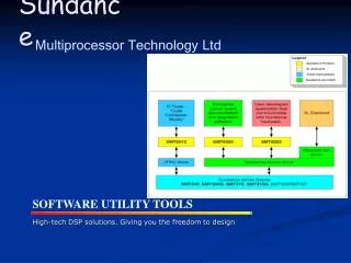
Sundance Firmware. Sundance uses a FPGA to implement the communication resources. Sundance has developed various communication resources such as PCI/ PCIe , 32-bit SHB, RSL…. Model Overview.

E N D
Sundance Firmware Sundance uses a FPGA to implement the communication resources. Sundance has developed various communication resources such as PCI/PCIe, 32-bit SHB, RSL…
Model Overview • Sundance uses modularity in its designs to improve reusability and maintainability. This approach creates a number of elementary blocks which are used to create the firmware.
Standard case of figure • The firmware is designed according to this model. • The FPGA is: • used to implement the communication interfaces, • connected to several peripherals. The role of the firmware is to allow these peripherals to exchange data, • connected to the peripherals via physical wires. • The peripherals may be zero or more processors, connectors or other components on the board. • The following diagram shows the FPGA connected to one processor, and two connectors. • The firmware comprises processor blocks,interface blocks, and connector blocks. All these blocks are interconnected with pre-defined signals. The connector and processor blocks are connected to the physical pins of the FPGA. • This is a standard case of figure.
Processor block • A processor block connects a processor to one or more interface blocks, allowing a processor to exchange data with interface blocks by accessing the resources inside the interface block. • The processor block translates the access made by the processor into a format that is understood by interface blocks. • The second main purpose of a processor block is to drive the event lines of the processor connected to it. Processor block uses triggers generated by interface blocks connected to it to generate events.
Interface block • The interface block implements a collection of addressable resources (registers, and memory space mainly) that can be read or written by a processor block. Interface blocks usually drive connector blocks. • By accessing these resources, a processor block can: • obtain status information about the interface block and the connector block attached to it, • control the state of the interface block and the connector block, • transfer data to and from the connector block. • Each interface block can be connected to one processor block, one connector block, and zero or more interface blocks.
Interface block • Processors might want to know when some condition is met inside the interface block. For example when the interface block has collected a certain number of words ready to be read. When such an event occurs, the interface block can generate a trigger. These triggers may be passed to other interface blocks and to processor blocks. • Some interface blocks, called event blocks, are dedicated to gather triggers and status information from other interface blocks, and to present them to a processor block. For example gathering the status and trigger information for all the XLINK interfaces in the system. Typically, these interface blocks allow the user to select which trigger conditions should be passed to the processor block. • To indicate to a processor that a trigger condition has been met, the processor block uses event lines to the processor. The processor block may drive these event lines when the interface blocks connected to it present a trigger condition.
Connector block • The connector block forms the interface to the pins of the FPGA that are going to the connectors via physical wires. • It is usually responsible for transmitting and receiving data to and from physical wires. • The connector block has an interface that allows you to: • Send data • Receive data • Control the connector block • Obtain status • All connector blocks work in a similar way but may drive the physical wires differently. They work at different speeds, and have different signals and characteristics. • Sundance provides a number of standard connector blocks, such as SHB and RSL. • Connector blocks are connected to interface blocks that drive them.
Implementation • This section describes the implementation of the model. • Each type of block (PB, IB, CB) has a standard interface. This interface is described in the files: • Smt_pkg.vhd. (PB IB, PB IB) • Chan_pkg.vhd.(IB CB, IB CB)
Processor block • Typically a processor connects to a peripheral using an address bus, a data bus, some control signals such as read, write and a few event lines. • In the case of Host processor via PCI/PCIe, the processor block decodes the address and the type of access made by the processor. It also generates address and control signals (read, write) used to drive the interface block. In return the interface block will provide data and triggers to the processor block. Triggers will be used by the processor block to generate events on the event lines of the processor. • The processor block forms the gateway between the processor and the firmware. • The connection between a processor and a processor block is not defined. It depends on the details of the processor. • The connection between a processor block and an interface block are defined by two specific types described below. • The signals provided by processor block to interface block are grouped in the type t_PB_IB_X. • The type t_PB_IB_X gathers: • a data bus • an address bus • some control signals such as read and write • a clock signal • a reset signal
Interface block • The interface block is connected to a processor block. Each interface block has a region of the processor block’s memory space associated with it. When an access is made in this memory range, the interface block is responsible for dealing with the access. The allocation of the range of memory of an interface block can be done by specifying the properties of this interface block. • The properties allow to specify the start and the end address of the interface block. This is defined in the type t_IBProperties. This is the way the memory mapping of interface blocks is done. • Interface blocks can implement functionality that is accessed by means of resources inside the memory space associated with it. These resources can be used to control the interface block, to obtain status and to communicate data with other blocks further down in the design. • The pre-defined collection of addressable resources implemented by an interface block is called an “interface” from a software point of view. The software interfaces are described in the SMT6400 package, and in the SMT6025 for the XLINK interface block and the IB_reg. • Interface blocks can be used to drive a connector block. • Interface block and connector block are connected via a “data type” connection.
Interface block • An interface block can also connect to another interface block to exchange trigger information, gathered under the type t_Trigger. This type gathers the following information: • Trigger: when the condition of the trigger is met a pulse is generated on this line. • Trigger_latch: this line becomes high when the condition is met. It stays high until it has been reset • Flag: the flag is usually the condition that generated the trigger. • Some interface blocks (called event blocks) implement functionality dedicated to the processing of these triggers. They gather status and triggers of other blocks in the design.
Another implementation of an Interface block could be an XLINK Event Block.
Memory mapping • The Processor block provides an address bus to interface blocks. The size of the address bus defines a memory space inside the FPGA addressable by the processor. • 32-bit addressing supported only. • The Interface blocks decode the address bus to know if they are being accessed by the processor block. Because this address bus can be “big”, it may be expensive in terms of logic to decode all of the bits that constitute it. To simplify the address decoding, the total memory space defined by the address bus is divided into compartments of a certain size. • Interface block will react only when an access is made within the range of compartment assigned to it. The size of the compartments is fixed to 1K addresses (2^10) in the Sundance’s firmware. • The start and the end compartment of an interface block are specified by configuring its properties. • The type t_IBProperties allows to specify the following parameters: • SHIFT_RIGHT: The bottom bits of the address bus provided by the processor block to be ignored when decoding the address. • SHIFT_LEFT : The top bits of the address bus provided by the processor block to be ignored when decoding the address. • STARTC: The number of the first compartment. • ENDC: The number of the last compartment.
Memory mapping • For example IB_0 requests two compartments, and the XLINK interface requests one compartment. The following diagram shows a possible memory arrangement for two imaginary interfaces (IB_0 and IB_3) and one XLINK interface. • (31-SHIFT_LEFT) - SHIFT_RIGHT= bits decoded • 2^ SHIFT_RIGHT = size of a compartment. • 2^(number of BITS DECODED) = number of compartments. • (END –START) + 1 = the number of compartments assigned to the Interface block. • For example the XLINK interface requests one compartment.
Connector block • A connector block forms the link to the physical pins of the FPGA. A connector block is connected to an interface block. • Connection between connector block and the physical pins of the FPGA are not defined as they are specific to each connector block. • Connection between connector block and interface block is of types X_chan_t and Y_chan_t. • NOTE: Sundance adopted the Diamond FPGA channel format to be able to port applications developed in Diamond FPGA into ISE projects and vice versa. • Connector blocks may also exchange information with the top level of the FPGA, such as clock or reset. These scalar connections are not defined as they are specific to each connector block. For the connector blocks that have them, they should all be following the same naming convention to facilitate reusability and block interchangeability.
Summary of FPGA Channels defined in the 3L Diamond Help file • Channels are used to connect blocks to other blocks: • Interface blocks • Connector Blocks • Custom Blocks. • A channel's unidirectional data transfer is achieved using two buses, X and Y, which carry signals in opposite directions between the communicating blocks. Each block must make sure to see the signals of the channels it can access as being synchronous to its own clock.
The Types • The following table describes the signals constituting each of the types used to implement the firmware.
SMT702 FIRMWARE • We assume you read and understood the documents given previously. • Processor block: Interface to the Pcie bus. XILINX_PCI_EXP_EP • Interface blocks :XLINKs, IB_Reg, IB_TOC • Properties: • IB_XLINK PROPERTIES in Smt7xx_XLink_Init_pkg. • IBToc PROPERTIES in IB_pkg. • IB_Reg PROPERTIES in IBReg_SMT7xx. • Connector blocks: • Register blocks: CB90_SMT7xx.vhd, CB_SMT702.vhd, CB_TOC_SMT7xx • Memory interface: DataPathDDR2FIFO.vhd. • serial interfaces.
SMT702 Firmware Memory mapping • The SMT702 memory mapping follows the table below.
SMT702 Firmware block: TOC • Number of XLINKs supported:4 max. • Address of Table of content (TOC):offset 1000 in hex from BAR1. • In the TOC, All values are in quad words (64 bits) • All offsets relative to the start of the FPGA are in bytes. • Addresses of TOC, TOD and devices are in no relationship with each other.
SMT702 Firmware block: Register Blocks • The register access is specified by a BAR address and offset values. software functions: • Write32(uintnBAR, uintnOffset, DWORD dword). • Read32((uintnBAR, uintnOffset). • Number of register Blocks: 2 sets. • 1. Register block SMT7xx: • Address at offset 0 from BAR1. • Implements status and control register for the board. • Firmware Reset control via software: • Reset function: ResetTIMs. (from SMT6026) • Reset Pulse used as the FPGA reconfiguration enable pulse. • The board is reconfigured with a bitstream from Flash hence, the board is removed from the PCIe devices list in the PC. • Interrupt status register, transparent to the user.
2. Register Block SMT702: • Address at offset 400 in hex from BAR1. • Implements specific functionalities proper to the SMT702, see a description in the SMT702 User Guide. • Reset: • Reset Pulse with a delay to give time to the Hardware to propagate the reset and clear all the IB FIFOs . • Does not reset the PCIe core to prevent loosing the board on the bus.
SMT702 Firmware block: XLINKs • The X-Link is a generic 32-bit interface that can be used with any communication resource to send data to and receive data from external devices. • See XLINK specifications document: • D000051S-spec.pdf • Supports DMA transfers to from the Host.
XLINK0: reserved to access the flash. Used bi-directionally. • XLINK1: Used bi-directionally. ADCA data path. Phase Shift Configuration for ADCA and ADCB • XLINK2: Used uni-directionally. ADCB data path.
SMT702 Firmware Blocks: Connector Blocks • Serrxtx : Provides Read/Write accesses to the flash. • DataPathDDR2FIFO: Provides access to: • the FIFO that collects both ADCA and ADCB data. • The SHB connector • It recaptures the data and places it in the FPGA clock domain via a FIFO. • CB90_SMT7xx: Provides the FPGA reconfiguration bitstream number and command. • CB90_SMT702: Provides • the path to set up the ADCs and PLL. • An interface to the system monitor feature of the Xilinx Virtex-5 FPGAs. • Also used to reset the XLINKs.
SMT712 FIRMWARE • We assume you read and understood the documents given previously. • Processor block: Interface to the Pcie bus. XILINX_PCI_EXP_EP • Interface blocks :XLINKs, IB_Reg, IB_TOC • Properties: • IB_XLINK PROPERTIES in Smt7xx_XLink_Init_pkg. • IBToc PROPERTIES in IB_pkg. • IB_Reg PROPERTIES in IBReg_SMT7xx. • Connector blocks: • Register blocks: CB90_SMT7xx.vhd, CB_SMT712.vhd, CB_TOC_SMT7xx • Memory interface: DACDDR2DataPath.vhd. • serial interfaces.
SMT712 Firmware Memory mapping • The SMT712 memory mapping follows the table below.
SMT712 Firmware block: TOC • Number of XLINKs supported:4 max. • Address of Table of content (TOC):offset 1000 in hex from BAR1. • In the TOC, All values are in quad words (64 bits) • All offsets relative to the start of the FPGA are in bytes. • Addresses of TOC, TOD and devices are in no relationship with each other.
SMT712 Firmware block: Register Blocks • The register access is specified by a BAR address and offset values. software functions: • Write32(uintnBAR, uintnOffset, DWORD dword). • Read32((uintnBAR, uintnOffset). • Number of register Blocks: 2 sets. • 1. Register block SMT7xx: • Address at offset 0 from BAR1. • Implements status and control register for the board. • Firmware Reset control via software: • Reset function: ResetTIMs. (from SMT6026) • Reset Pulse used as the FPGA reconfiguration enable pulse. • The board is reconfigured with a bitstream from Flash hence, the board is removed from the PCIe devices list in the PC. • Interrupt status register, transparent to the user.
2. Register Block SMT712: • Address at offset 400 in hex from BAR1. • Implements specific functionalities proper to the SMT712, see a description in the SMT712 User Guide. • Reset: • Reset Pulse with a delay to give time to the Hardware to propagate the reset and clear all the IB FIFOs . • Does not reset the PCIe core to prevent loosing the board on the bus.
SMT712 Firmware block: XLINKs • The X-Link is a generic 32-bit interface that can be used with any communication resource to send data to and receive data from external devices. • See XLINK specifications document: • D000051S-spec.pdf • Supports DMA transfers to from the Host.
XLINK0: reserved to access the flash. Used bi-directionally. • XLINK1: Used to send the data pattern to DAC A. • XLINK2: Used to send the data pattern to DAC B.
SMT712 Firmware Blocks: Connector Blocks • Serrxtx : Provides Read/Write accesses to the flash. • DACDDR2DataPath : Provides access to: • the FIFO that contains both DACA and DACB data pattern. • The SHB connector. • The DDS. • CB90_SMT7xx: Provides the FPGA reconfiguration bitstream number and command. • CB90_SMT712: Provides • the path to set up the DACs. • An interface to the system monitor feature of the Xilinx Virtex-5 FPGAs. • Also used to reset the XLINKs.