Download

1 / 38
380 likes | 594 Vues
Low charge button and stripline BPM electronics based on MicroTCA. Development status of the first MicroTCA based BPM system. Bastian Lorbeer, DESY, MDI DITANET workshop CERN, 17 January , 2012. Outline. OUTLINE FLASH 1 and FLASH 2 Requirements Concept and Signals

E N D
Low charge button and stripline BPM electronics based on MicroTCA Development statusof thefirstMicroTCAbased BPM system Bastian Lorbeer, DESY, MDI DITANET workshop CERN, 17 January, 2012
Outline • OUTLINE • FLASH 1 and FLASH 2 • Requirements • Conceptand Signals • Acquisition • Evaluation • Summary And Outlook
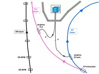
Striplineandbuttoninstalled BPMs in FLASH button BPM New uTCAbased BPM electronics will successivelyreplaceold VME based systems in FLASH stripline BPM cavity or re-entrant cavity BPM accelerating modules bunch compressors gun bypass line FEL beam undulators matching section collimator section matching section dump 5 different button BPM typesdeliver different amplitudeand signalshape 2 different typesofstripline BPM Source: Drawing from Nicoleta Baboi, DESY, MDI
Performance ofinstalled BPMs at FLASH Stripline BPMs button type BPMs Forbothtypesof BPMs theresolutionissufficient down to a charge ca. 0.5nC -> belowthislevelnewelectronicsorimprovement in the existent arenecessary Source: Measurements by Nicoleta Baboi, DESY, MDI
Button / Stripline BPM for FLASH 2 Extractionregion wheremany BPMs will beinstalled Extraction top view FLASH 2 Button andstripline BPMs will beequippedwithMicroTCA systems
I 1.0-0.111s (XFEL 200s) bunch spacing t Relevant parametersforelectronicsdesign The FLASH2 specifications are compatible with XFEL requirements I Duty cycle ~ 0.8% (XFEL 0.65%) 1-9 mA 100ms t I 800s (XFEL 650s) Ipeak~ 2.5 kA Macro-pulse duration t Source: Dirk Nölle, Boris Keil, Winfried Decking: „The European XFEL Beam Position Monitor System”, Conceptual Design Report Document 3: Requirements & Interface Definition Rev. 1.00, June 15, 2010
Conceptualsystem design SIS8300 10channel ADC board U1 U2 +Stripline BPM Examplefollows: Warm button type XFEL RTM lowcharge Peak detector electronics Housingis a MicroTCAcrate Delay upto 100ns, Not fix yet ! RF cable 3/8“ Length < 30m Combiner type: broadband
Button BPM simulationandmeasurement feedthroughs spectraof buttonsignal after cable Diameter: 40.5 mm Button size: 17 mm • monitorconstant SDUMP: Measured : 11.29 ± 0.72 mm Simulated : 10.61 mm Dirk Lipka et. al.: „Button BPM Development for the European XFEL”, Proceedings of DIPAC2011, Hamburg, Germany, MOPD19, Measurement data from 1. May 2011 at SDUMP
Signal of horizontal plane, delay: ~55ns Cable length: ~80m Typicalbutton BPM receiverInput Signal / Charge sweep Measurement at SDUMP on 1 May 2011 Position information U1, U2 Charge sweep Position ~ 3.75mm 100mV ~ 100pC minimumofbunchsignal forcentered beam isdisplayedhere ! 55ns
TypicalStripline BPM receiverinputsignal Signal hereshownforonestripline Filteredwith a 8 order low pass filterat 500MHz Betteruse a flat time responsefilterhere ! 1.35ns Striplineparameters beamlinedia = 34 mm striplinelength= 200.5mm cable type / length = 3/8‘‘ Acome / ~20 m Monitor constant= 20mm
VME vs. MicroTCA VME Numberofnewdevelopmentsisdecreasing,salesare still constant Bus technologyhasspeedlimitations Wide bussescreate a lotofnoise in analog channels But, a lotof I/O modulesareavailable Nostandardmanagement on cratelevel Nomanagement on modulelevel So farnoextensionbussurvived Onedamagedbuslinestops a wholecrate Addressandinterruptmisconfigurationsarehardtofind MicroTCA Scaleable modern architecture From 5 slot µTCA … full mesh ATCA Gbitserialcommunication links High speed and no single point of failure Standard PCIe, Ethernet (, SRIO) communication Redundant systemoption 99.999% availability is possible Welldefinedmanagement A must for large systems and for high availability Hot-swap Safe against hardware damage and software crashes Courtesy: Kay Rehlich, MCS, DESY
MicroTCAsystemscurrentlyusedat DESY-MDI 6 slots Laboratory cratesystem 19‘‘ productioncratesystem 12 slots Back Front Zone 3 connector Digitizer AMC timing analog frontend RTM HD & VGA CPU System specsarebased on the PICMG standard(MTCA 4.0 for Physics)
LCBPM RTM RearTransition Module Zone 3 connector: Input 1 Test pulse in Input 2 Test pulse out Externalclk TTL Gate MPS Power supply RTM LCBPM made by MDI1 / FEB
RTM onechannel onechannelforone plane activetemperature Stabilizationofdiode 31.25dB range 0.25 dB steps To ADC buffers On digitizer board via Zone 3 connector Gain ~ 36dB
Typical Output signalsof RTM Signals fromone plane combined after a delaylineof 14 m 62ns Input signalto front end 100ns delayforsecond pulse generatedwith AWG resembleszerooffsetsignal Output signal after peakdetectortestport 750mV forfirst pulse Fromhere: calculationofoffsetposition ! First pulse: informationfor U1 Second pulse: informationfor U2
ADC inputcircuitryandclockingscheme Clockdividers: Phase offset Programmabledelay ADC buffer Clockdistributionforvariousclockingschemes chip w/ 2 ADCs Traces to ADC boardare lengthcompensated on SIS 8300-V2 125MSPS 10 channels Optional Clockingfrom: externalclocksfedfrom RTM, or backplane Block diagram: SIS8300 μTCA FOR PHYSICS DigitizerUser Manual, SIS8300-M-1102-2-V211.doc asof 05.08.11
ADC / buffernoiseof DC coupledchannels measurementwith ~100Ωinputtermination Typicaltimetraceofsingle ADC channel: all channels on theboard: in mV peak-peak! counts Plottedfor all 10 channels All channelshave a noise band lessthan 1.2mV – approximately 11/12 Bits These arethe DC coupledchannels !!
Noise of RTM and AMC in cratewith 50 Ohm inputload ADC channelsofone plane (e.g. horizontal plane) all ADC channelsofdigitizerboard All channelshave a noise band lessthan 1.5mV –still ca.10 Bits
Currentlaboratorysetup ArbitraryWaveform Generator: 10Bit Resolution 12GS/s (-3dB @ 3.5GHz) Free running clock at 125MHz at the moment Access servers Provided by MCS, DESY bunchsignals Input signal Trigger Dicharge pulse raw data out Read out with a MATLAB tool from server
A train of output pulses Input signal - combined signal of two buttons in one plane Example: Signal levelscorrespondto a 40.5 mm button BPM (17 mm button) @ 30 pC closetothecenter pos 2 pos 1 Performance data not yet calculated from pulse train output!
Summary & Outlook • OUTLOOK • More detailed analysis of available data • More lab tests (position sweep for different charges) • Evaluation in machine of the system to come Feb/ Mar 2012 • Improvements in the power supply on RTM and signal conditioning • Development of correction tables for individual charges • Possible switching to 250MSPS ADC with 14Bits on the acquisition card • Series production of redesign at the end of summer 2012 • Development of FPGA firmware to process data on acquisition card • Correctionalgorithm for large offsetsofthebeam • SUMMARY • Measureseachbunch in trainwithrepetition rate of 222ns • Dynamic rangefrom 0.1 to 1nC • Calibrationwith 10 Bit resolutioninputsignals in the lab • Online testingpossiblebetweenmacropulses • Free runningmodeandsynchronousmode • Timing andclocksdeliveredbythethemachine in thesynchronousmode
Jorgen Lund-Nielsen, Rudolf Neumann, Frank Schmidt-Föhre, Nicoleta Baboi, Dirk Nölle, Petr Smirnov, Peter Göttlicher, Bart Faatz, andmanyothers Thanks
Signal in thereceiveranddischargepath After first LNA After second LNA After dischargerand buffer After dischargertestport signal
Power supplynoise Measuredoutsidethecratewithlaboratory DC supply 8V power supply ext DC: Vrms= 28uVrms Vpkpk= 220uV Measurement limit: Vrms= 13uVrms Vpkpk= 100uVpkpk Measured in a bandwidth B= 1GHz !!!
Low noiseamplifieroutputnoise Measured outside thecratewithexternal DC supply Evalboard LNA: Vrms= 242uVrms Vpkpk= 1.7mV Measurement limit: Vrms= 13uVrms Vpkpk= 100uVpkpk Measured in a bandwidth B= 1GHz !!!
LNA evalboard vs. LNA PCB Evalboard *100 andexternalsupply LNA on PCB *100 andcratesupply 1.8us repetitive spikesfromcratesupply 555kHz Nakedcratebrings 3.6us repetitive ripple 277kHz Behind DCDC crate
Bandwidthoffrontend „RF part“ -3dB cornerat ~ 330MHz Flat time response !
FEMTO preamprisetime / bandwidth Measuredwith AWG square 1000 MeasuredwithJorgenspulser
Synchronisation withMachine Timing • Features • Both transmitter and receiver functionality • Delivers clocks and triggers through front panel and backplane. • 8 M-LVDS signals to the backplane • Main frequency is 1.3 GHz • Derived frequencies are divided from the main frequency, and synchronized in phase • Clock outputs are adjustable in stepsof 100 ps • Single SFP for optical communication • ~25 W power consumption • Purpose • Distribute clocks and trigger information to the whole • accelerator system and experiments. • Deliver the 1.3 GHz main RF-frequency and other derived • frequencies. • Synchronize the clock-phases and keep them drift free, with a • total jitter: <5 ps (RMS). • Deliver clocks and triggers through the backplane and through • the front panel. • Cost efficiency Courtesy: Attila Hidvégi, Stockholm University Physics Departement, Rev 0.1.2
Historyof BPMs at DESY SEDAC Module anno 1985, Rudolf Neumann, Jörg Neugebauer uva. TektronixScanconverter anno 1976, peopleinvolved: Franz Peters, Rudolf Neumann XFEL BPM prototype in 2007, Thomas Traber, projectassignedto PSI Wendt Elektronik, VME basedsince 1995 andearlier in operationat FLASH w/ remote accesssince 2005, electronicswithmanymodificationsandimprovements by Jorgen Lund-Nielsen and Wolfgang Riesch