Section 4 Printed Board Characteristics
Section 4 Printed Board Characteristics. IPC Designer Certification Study Guide. Section 4.1 Board and Assembly Panelization. Printed Board Characteristics.

Section 4 Printed Board Characteristics
E N D
Presentation Transcript
Section 4Printed Board Characteristics IPC Designer Certification Study Guide
Section 4.1 Board and Assembly Panelization Printed Board Characteristics
The definition of a panel is a rectangular sheet of base material, of predetermined size, that is used for the processing of one or more printed boards, and when required, one or more test coupons. There are two types of panels: one is for the production of the bare printed board, the other is for the production of the board assembly. Fig 3-29 Board and Assembly Panelization - 4.1
The development of each panel has a set of rules to follow that make the process of building boards and assemblies more productionized. Some of the rules deal with the extra material that is required around the border and the room between each of the boards. Techniques for separation must also be taken into account. SM782 Fig 3-14 Board and Assembly Panelization - 4.1
Board fabrication companies try to use the largest panel possible to make the most efficient use of the manufacturing process and ease printed board handling. The size is usually based on the common size sheet in the market place. In the United States the common sheet size is 36 x 48 inches; in Europe and Asia the common sheet size is 1 meter square. Board and Assembly Panelization - 4.1
The designer should be aware of the board size that the manufacturer of choice uses in production so they will be able to optimize the board to panel yield and cost relationships. There was a time that it was sufficient to simply take the board dimensions, divide them into the fabrication dimensions, and allow sufficient room for borders. The issues are more complex today since many assembly companies do not want to assemble boards in individual format. They also want boards delivered in panels. Board and Assembly Panelization - 4.1
The use of the largest panel in board fabrication provides the most effective labor cost per unit area. The industry processes panels. Being able to get twelve boards on a panel instead of six (3 x 4 versus 2 x 3), immediately increases the yield by 100%. The most common panel in the US is 457 x 610mm [18 x 24 inches]. Board and Assembly Panelization - 4.1
Some of the processing equipment can accommodate larger panels, however, human factors such as strength, reach and control, preclude the use of much larger panels. Borders and margins are usually required and range between 9.5 to 38mm [.38 to 1.5 inches]. Board and Assembly Panelization - 4.1
Tooling holes, coupons, and other manufacturing entities such as serialization or customer control numbers are also contained in the borders of the panel. 2222 5.2.1.1 Board and Assembly Panelization - 4.1
Separating boards or assembly panels from the fabrication panel varies depending on the next use of the board, material, the shape and size, and volume of production. Higher volume production tends to utilize punching or blanking dies to excise boards, or assembly panels, from fabrication panels. Board and Assembly Panelization - 4.1
Fixturing is relatively expensive and requires careful maintenance to assure good quality board edges. Freshly sharpened blanking dies will generally provide a relatively smooth board edge. However, as the die is used, the board edges tend to roughen with exposed broken fibers. SM782 3.6.4.5 Fig 3-30 Fig 3-31 Fig 3-32 Board and Assembly Panelization - 4.1
Scoring and routing are two of the most common methods used for excising printed boards or assembly panels. The easiest way to separate the board is to score each side with a diamond grinder and break the boards or panels apart. The board must be square or rectangular, in shape, in order to use scoring and care is required to not have conductors too close to the scored area, as the score wheel is chamfered. Board and Assembly Panelization - 4.1
2222 5.3.1 It is required to score the board on each side to approximately 1/3 of the thickness. If the boards are routed, an amount should be left between the boards to accommodate the router bit. This is usually 4.8, 5.0 or 6.3mm [.19, .20, or .25 inches]. When boards are routed the edges are usually very smooth. Scoring leaves the edges a bit rough where the remaining board thickness has exposed broken fibers. Fig 5-2 Table 5-2 SM782 3.6.4.5 Fig 3-30 Fig 3-31 Fig 3-32 Board and Assembly Panelization - 4.1
Assembly panels also require borders but these are usually related to the conveyor of the assembly machines. The borders also contain tooling holes or fiducials. Borders are only on opposite sides of the panel where the conveyer grips the panels, however, some material is necessary at the leading and trailing edge where the final board comes close to the panel edge. Extra 4.1b Board and Assembly Panelization - 4.1
The relationship of the final board and the two panel concepts must be understood and considered in the design to maximize the manufacturing operations. Some companies find it useful to develop a panelization drawing in order to maintain control of the tooling features of the assembly panel. Extra 4.1 Board and Assembly Panelization - 4.1
Section 4.2 Tolerancing Methods Printed Board Characteristics
Atoleranceis the total amount that a specific dimension is permitted to vary. Therefore a toleranced dimension is a dimension that has a specified amount of variance that is acceptable. These principles are intended to allow for interchangeability of parts and the form, fit, and function of mating products. Tolerancing Methods - 4.2
A dimension may also be specified without a tolerance. In this instance the term basic is assigned to the dimension or the dimensional location. The variation of the basic dimension then controls the variation usually in relation to some datum or datum reference. 2221 5.4.1 Tolerancing Methods - 4.2
There are many methods of dimensioning and tolerancing for mechanical parts, all of which are defined in ASME Y14.5M. A printed board assembly, although performing an electrical function, has many mechanical attributes that require dimensioning and tolerancing. These include the location of the parts, the features (holes, conductors, legend, etc.), and board outline in relation to the datum from which dimensions are taken. Tolerancing Methods - 4.2
Physical characteristics are also mechanical in nature and require dimensions and tolerances. Examples are parts, diameter of holes, cutouts or notches, plating thickness, in fact any feature that requires a control to assure the final product is consistent from lot to lot. 2221 5.4.1 Tolerancing Methods - 4.2
All the methods in ASME Y14.5M work, but it should be recognized that some work better than others and some methods cost less to inspect or evaluate the final product than others. One of the main considerations in evaluating a system for dimensioning or tolerancing is to recognize that every mechanical feature has a maximum material condition (MMC) and a least material condition (LMC). Tolerancing Methods - 4.2
2615 3.3.1 Although a tolerance can be expressed as a variation from nominal, unless that dimension is the true target value it is better to specify the range for the upper or lower limit of the tolerance. At times it may be necessary to provide a dimension that is only specified as a maximum (MMC) or minimum (LMC). But, it should be remembered that the opposite condition can also result. 2615 3.3.4 Table 3-1 Table 3-2 Table 3-3 Tolerancing Methods - 4.2
Plated-through holes are usually specified as needing a minimum of 20 microns [.0008”] of plated copper in the hole. This requirement is intended to establish the reliability of the plated-through hole to serve its function as a conductor. Many holes are also used as component mounting holes, therefore another dimension must be specified to provide the hole diameter range. Tolerancing Methods - 4.2
A hole that is specified to be 1.0-.85mm [.040”-.034”] has a range of 0.15mm [.006”] from the maximum material condition (when the hole is at its smallest) to the least material condition (when the hole is at its largest). The plating thickness on each side wall of the hole must be included in those requirements. Thus, the board fabricator drills the hole slightly larger to allow for the plating to reduce the drilled diameter. 2221 9.2.1.1 9.2.2.2 Table 9-5 2615 3.3.4 Tolerancing Methods - 4.2
Location of the feature is also important. Most holes or other critical features are located at a basic intersection of some orthogonal grid. That point has no tolerance and is expressed as being the true position of the feature (basic location). The tolerance is then applied as a zone about that location in which the center of the feature must be located. Tolerancing Methods - 4.2
Bilateral tolerance zones are square (plus or minus from true position); geometric tolerance zones (diameter or radius of true position) are circular. Both systems work, however, the geometric method is preferred. (Will discuss in next section). 2221 5.4.1 2221 Fig 5-4 2221 5.4.2 Tolerancing Methods - 4.2
Section 4.3 Hole Types and Their Tolerances Printed Board Characteristics
Dimensions and tolerances are important characteristics for determining the location of holes as well as their final size. Dimensioning principles are established by ASME Y14.5M. This document contains a lot of good information which is followed in mechanical dimensioning strategies. Hole Types andTheir Tolerances - 4.3
There are very few examples of printed boards or electronic components so the organizations that develop those standards have adopted the ASME Y14.5M principles and provided additional information for their users; i.e., IPC-2615, EIA 100, and JEDEC 95. All support the idea of datums, datum features, and the various dimensioning systems to allow manufacturing to produce consistent, interchangeable parts. Hole Types andTheir Tolerances - 4.3
The principles for hole location consists of three different methodologies. These are: • The bilateral methoddevelops a tolerance zone made up of a plus or minus from a true position or location. This zone is a square when the plus or minus dimensions are equal. Hole Types andTheir Tolerances - 4.3
The positional tolerance zonea circular zone that essentially is equal to the hypotenuse of the right triangle formed by the bilateral method (which provides for additional variation capability in the North, South, East and West sectors of the zone). The theory being that if a feature could be off true position on the diagonal of the square there isn’t much difference if it were off along the X Y coordinate lines. Hole Types andTheir Tolerances - 4.3
A third method allows additional misalignment in that the requirement is specified as being applicable at Maximum Material Condition (MMC). Since holes are at their least dimension they could theoretically move a small additional amount from true position considering the difference between the maximum and minimum hole diameter. Dimensions of this type are expressed as being a specific diameter or radius of true position (DTP). 2221 5.4.1 Fig 5-4 Hole Types andTheir Tolerances - 4.3
Currently holes in boards are produced using mechanical drilling. But, new techniques are being explored that employ lasers or plasma etching. Drill sizes come in increments of 0.05mm [.002"]. Usually the manufacturer prefers to select the drill to be used in achieving the desired result. Extra 4.1c Hole Types andTheir Tolerances - 4.3
2222 9.2.1.2 Therefore, most documentation principles require that the final hole size is specified. It is best to specify a range for the hole diameter, as opposed to the indication of a plus or minus tolerance from some imaginary nominal dimension. 9.2.2 9.2.2.2 Fig 9-3 Table 9-5 Table 9-3 Table 9-2 Table 9-4 Hole Types andTheir Tolerances - 4.3
Once the maximum and minimum diameters are identified the manufacturer can select the appropriate drill to achieve the desired end result considering material shrinkage or plating thickness in the hole. The designer does, however, need to have an idea of what drill might be used especially for determining the annular ring for internal layers of a multilayer board. The acceptance requirements are based on measuring the minimum annular ring from the wall of the drilled hole. 2222 9.3 Table 9-7 Hole Types andTheir Tolerances - 4.3
Hole sizes are either provided in inches or in millimeters. Drill sizes are in millimeters and using that method is preferred on all new designs according to the international grid identified in IEC 97. This document states that all features should be on a 0.5mm or 0.05mm grid as opposed to the original grid of the past which was .100", .050", .025", or increments of .005". Hole Types andTheir Tolerances - 4.3
It is not recommended to intermix grids on the same design. Rather, the best solution is to select a grid that will accommodate the majority of the components. Since component manufacturers are all supporting metric dimensioning, most design facilities are switching their libraries to prepare for the day when everything is in metric dimensions. 2222 9.3 Table 9-7 Hole Types andTheir Tolerances - 4.3
Through-holes come unsupported, or as plated holes (supported). Plated-through holes go through the entire board thickness. There are also blind via holes (open to one side), and buried vias (inside the board and not exposed to the outside). All vias are plated holes. All holes should use the same system for describing their size limits and their location. 2221 9.2.7.3 Table 9-4 Table 9-5 Hole Types andTheir Tolerances - 4.3
Section 4.4 Conductive Pattern Location to Datum References Printed Board Characteristics
A datum is the theoretically exact point, axis or plane, that is the origin from which the location of geometric characteristics of features of a part are established. For printed boards and printed board assemblies the datum is usually established by some feature of the board. The datum feature is the actual feature of a part that is used to establish a datum. Conductive Pattern Locationto Datum References - 4.4
Datum features can be holes, tooling holes, lands, symbols, fiducials, or any part of the board that the designer wishes to use in order to control the board and/or assembly characteristics. 2615 3.3.2 Fig 3-1 Fig 3-2 Conductive Pattern Locationto Datum References - 4.4
Characteristics that demand very fine controls may require the use of localized datum features. Datum features are used to establish the datum reference. A datum reference is a point, line, or plane that is used to locate the pattern or layer for manufacturing, inspection purposes, or both. 2221 5.4.3 Fig 5-5A thru Fig 5-5E Fig 5-6 Conductive Pattern Locationto Datum References - 4.4
Typically, the designer establishes the single board image as s/he develops the circuitry and positions all of the components. The board manufacturer, however rarely produces one board at a time. Board manufacturers panelize the one-up board and position as many as possible on a production panel. Conductive Pattern Locationto Datum References - 4.4
The assembler also prefers to work in a panel format. An individual board is positioned several times on an assembly panel; several assembly panels are positioned on the board fabrication panel. It is for these obvious reasons that the description of the individual board feature locations must be clear and unambiguous. Conductive Pattern Locationto Datum References - 4.4
Boards are positioned in many different orientations (work and turn) to accommodate plating uniformity or placement sequencing, thus the relationship of the original datum reference is critical in order to maintain the board feature location perspective. Extra 4.1 2221 5.4.3.1 Fig 5-7 Conductive Pattern Locationto Datum References - 4.4
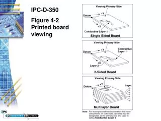
Most designs are accomplished with the individual board being viewed having the primary side up, or facing the viewer. The primary side of the board is established by the designer and is usually the side that contains the most or the most complex components, however, the selection can be based on testing or inspection focus. Conductive Pattern Locationto Datum References - 4.4
Once established, the first conductive layer on this side is labeled layer one. Thus, layer one also faces up. This orientation and the datum features establish three mutually perpendicular planes. The names of these planes are primary, secondary, and tertiary. Conductive Pattern Locationto Datum References - 4.4
2221 5.4.3 The primary datum plane is opposite the primary side of the board. When viewing layer one, which would essentially be the top of the board, the last layer would be on the bottom of the board; it becomes the primary reference plane from which any Z axis dimensions should be defined. Fig 5-5A thru Fig 5-5E Fig 5-6 D325 4.2 Table 4-1 Table 4-2 Conductive Pattern Locationto Datum References - 4.4
The secondary and tertiary datums then become the X and Y axis of the board. As such they control the positioning of the pattern and all other features, conductive, nonconductive, circuitry, masking or legend. It is a requirement that the secondary datum reference be located with the feature that identifies the point of origin of all the dimensional characteristics (i.e. coordinate zero). Conductive Pattern Locationto Datum References - 4.4
There are cases where only one datum is necessary for inspection or definition of dimensions and tolerances. If only one datum reference is established it would be the secondary datum, however, angular deviation could not be specified nor could Z axis variation from true perpendicular. These conditions may only affect acceptance of the final product and may not be necessary for the manufacturer or assembler to interpret the location or dimensional requirements. 2221 5.4.3 Fig 5-5A thru Fig 5-5E Fig 5-6 Conductive Pattern Locationto Datum References - 4.4