Download
1 / 48
820 likes | 1.81k Vues
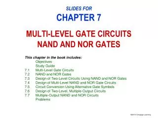
This chapter in the book includes: Objectives Study Guide 7.1 Multi-Level Gate Circuits 7.2 NAND and NOR Gates 7.3 Design of Two-Level Circuits Using NAND and NOR Gates 7.4 Design of Multi-Level NAND and NOR Gate Circuits 7.5 Circuit Conversion Using Alternative Gate Symbols

E N D
This chapter in the book includes: Objectives Study Guide 7.1 Multi-Level Gate Circuits 7.2 NAND and NOR Gates 7.3 Design of Two-Level Circuits Using NAND and NOR Gates 7.4 Design of Multi-Level NAND and NOR Gate Circuits 7.5 Circuit Conversion Using Alternative Gate Symbols 7.6 Design of Two-Level, Multiple-Output Circuits 7.7 Multiple-Output NAND and NOR Circuits Problems SLIDES FORCHAPTER 7MULTI-LEVEL GATE CIRCUITSNAND AND NOR GATES
In this unit, we will use the following terminology: • AND-ORcircuit means a two-level circuit composed of a level of AND gates followed by an OR gate at the output. • Sum-of-products(SOP): AB’+ACD+ABC’…… • OR-ANDcircuit means a two-level circuit composed of a level of OR gates followed by an AND gate at the output. • Product-of-sums(POS): (A+B’)(A+C+D)(A+B+C’)…… • OR-AND-OR circuit means a three-level circuit composed of a level of OR gates followed by a level of AND gates followed by an OR gate at the output. • Circuit of AND and OR gates implies no particular ordering of the gates; the output gate may be either AND or OR. Multi-Level Gate Circuits
Multi-Level Gate Circuits • What’s the concerned issues from a logic designers: • Number of gates • Gate inputs • Level of a circuit • a. Cascaded circuit will increase the gate-delay • b. and also the cost. • c. gate-delay will slow down the operation of a digital system
Each node on a tree diagram represents a gate, and the number of gate inputs is written beside each node. Tree Diagrams
Find a circuit of AND and OR gates to realize f (a, b, c, d) = Ʃ m(1, 5, 6, 10, 13, 14) Consider solutions with two levels of gates and three levels of gates. Try to minimize the number of gates and the total number of gate inputs. Assume that all variables and their complements are available as inputs. First, simplify f by using a Karnaugh map. Example
This leads directly to a two-level AND-OR gate circuit. Figure 7-4
Factoring yields f = c′d(a′ + b) + cd′(a + b)
Asolution with an AND gate at the output Both of these solutions have an OR gate at the output. A solution with an AND gate at the output might have fewer gates or gate inputs. A two-level OR-AND circuit corresponds to a product-of-sums expression for the function. This can be obtained from the 0′s on the Karnaugh map as follows: f′ = c′d + ab′c′ + cd + a′b′c (7-3) f= (c + d)(a′ + b + c)(c′ + d′)(a + b + c′) (7-4) Equation (7-4) leads directly to a two-level OR-AND circuit. 要直接從SOP轉POS, 可以取函數之補數, 再以DeMorgan’s Laws轉成POS來獲得.
To get a three-level circuit with an AND gate output, we partially multiply out Equation (7-4) using (X + Y)(X + Z) = X + Y Z: f= (c + d)(a′ + b + c)(c′ + d′)(a + b + c′) (7-4) f= [c + d(a′ + b)][c′ + d′(a + b)] (7-5) Equation (7-5) would require four levels of gates to realize; however, if we multiply out d′(a + b) and d(a′ + b), we get f= (c + a′d + bd)(c′ + ad′ + bd′) (7-6) which leads directly to a three-level AND-OR-AND circuit.
ORgate output ANDgate output
For this particular example, the best two-level solution had an AND gate at the output, and the best three-level solution had an OR gate at the output. In general, to be sure of obtaining a minimum solution, one must find both the circuit with the AND-gate output and the one with the OR-gate output. Figure 7-6 Figure 7-5
7.2 NAND gates and NOR gates In this section we will define NAND and NOR gates. Logic designer frequently use NAND and NOR gates because they are faster and use fewer components than ANDor OR gates.
Toshiba announced NAND flash at the 1987 International Electron Devices Meeting. It has reduced erase and write times, and requires less chip area per cell, thus allowing greater storage density and lower cost per bit than NOR flash; it also has up to ten times the endurance of NOR flash. A USB memory
NAND gates Figure 7-8(a) shows a three-input NAND gate. The small circle (or “bubble”) at the gate output indicates inversion, so the NAND gate is equivalent to an AND gate followed by an inverter, as shown in Figure 7-8(b). The gate output is F = (ABC)′ = A′ + B′ + C′ Figure 7-8: NAND Gates
NOR gates Figure 7-9(a) shows a three-input NOR gate. The small circle at the gate output indicates inversion, so the NOR gate is equivalent to an OR gate followed by an inverter. The gate output is F= (A + B + C)′ = A′B′C′ Figure 7-9: NOR Gates
Functionally Complete Set of Gates AND 和NOT可以用來實現OR之功能 AND and NOT are a functionally complete set of gates because OR can also be realized using AND and NOT: Section 7.2 (p. 196)
NAND Gates Similarly, any function can be realized using only NAND gates (Similarly, any function can be realized using only NOR gates) Figure 7-10: NAND Gate Realization of NOT, AND, and OR NAND可以用來實現NOT,OR和AND之功能, logic designer prefer this.
Design of Two-Level NAND-Gate Circuits A two-level circuit composed of AND and OR gates is easily converted to a circuit composed of NAND gates or NORE gates using F = (F′)′ and then applying DeMorgan′s laws: (X1 + X2 + … + Xn)′ = X1′ X2′…Xn′ (7-11) (X1 X2…Xn)′ = X1′ + X2′ + … + Xn′ (7-12) Section 7.3 (p. 197)
Design of Two-Level NAND-Gate Circuits The following example illustrates conversion of a minimum sum-of-products form to several other two-level forms: F= A + BC′ + B′CD = [(A + BC′ + B′CD)′ ]′ AND-OR = [A′ • (BC′)′• (B′CD)′]′ NAND-NAND = [A′•(B′ + C) • (B + C′ + D′)]′ OR-NAND = A + (B′ + C)′ + (B + C′ + D′)′ NOR-OR Section 7.3 (p. 197)
Design of Two-Level NOR-Gate Circuits If we want a two-level circuit containing only NOR gates, we should start with the minimum product-of-sums form for F instead of the minimum sum-of-products. After obtaining the minimum product-of-sums from a Karnaugh map, F can be written in the following two-level forms: F= (A + B + C)(A + B′ + C′)(A + C′ + D) OR-AND = {[(A + B + C)(A + B′ + C′)(A + C′ + D)]′ }′ = [(A + B + C)′ + (A + B′ + C′)′ + (A + C′ + D)′]′ NOR-NOR = (A′B′C′ + A′BC + A′CD′)′ AND-NOR = (A′B′C′)′ • (A′BC)′• (A′CD′)′ NAND-AND Section 7.3 (p. 197)
The other eight possible two-level forms are degenerate in the sense that they cannot realize all switching functions. Consider, for example, the following NAND-NOR circuit: From this example, it is clear that the NAND-NOR form can realize only a product of literals and not a sum of products. • NAND and NOR gates are readily available in IC form .So two • commonly used circuit is NAND-NAND or NOR-NOR.
Design of Minimum Two-Level NAND-NAND Circuits Procedure for designing a minimum two-level NAND-NAND circuit: 1. Find a minimum sum-of-products expression for F. 2. Draw the corresponding two-level AND-OR circuit. 3. Replace all gates with NAND gates leaving the gate interconnection unchanged. If the output gate has any single literals as inputs, complement these literals. Figure 7-12: AND-OR to NAND-NAND Transformation
Design of Minimum Two-Level NAND-NAND Circuit F = l1 + l2 + • • •+ P1 + P2 + • • • F = (l1′l2′ • • •P1′P2′ • • •)′ Figure 7-12: AND-OR to NAND-NAND Transformation
Design of Minimum Two-Level NOR-NOR Circuit Procedure for designing a minimum two-level NOR- NOR circuit: 1. Find a minimum products-of-sumexpression for F. 2. Draw the corresponding two-level OR-AND circuit. 3. Replace all gates with NOR gates leaving the gate interconnection unchanged. If the output gate has any single literals as inputs, complement these literals.
Design of Multi-Level NAND- and NOR-Gate Circuits The following procedure may be used to design multi-level NAND-gate circuits: • Simplify the switching function to be realized. • Design a multi-level circuit of AND and OR gates. The output gate must be OR. AND gate outputs cannot be used as AND-gate inputs; OR-gate outputs cannot be used as OR-gate inputs. • Number the levels starting with the output gate as level 1. Replace all gates with NAND gates, leaving all interconnections between gates unchanged, leave the inputs to levels 2,4,6,… unchanged. Invert any literals which appear as inputs to levels 1,3,5,… 對於多級電路之設計: (1)若是最終output為OR gate, 以Multi-Level NAND-gate 執行之。 (2) 若是最終out put為ANDgate,以 Multi-Level NOR-gate 執行之。
EX:F1= a′ [b′+c(d+e′)+f′g′]+hi′j+k • Steps: • Realize the function • with AND-OR • Replacing all gate with • NAND • 2,4,6,…leave unchanged • 1,3,5… invert literals Multi-Level Circuit Conversion to NAND Gates
Alternative Gate Symbols Logic designers who design complex digital systems often find it convenient to use more than one representation for a given type of gate. For example, an inverter can be represented by Section 7.5 (p. 201)
Equivalent gate symbols based on DeMorgan′s Laws Alternative Gate Symbols
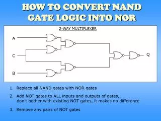
If AND and OR gates don’t alternate? EX: AND-OR Circuit to NAND Gates
Design of Two-Level, Multiple-Output Circuits Solution of digital design problems often requires the realization of several functions of the same variables. Although each function could be realized separately, the use of some gates in common between two or more functions sometimes leads to a more economical realization. Example: Design a circuit with four inputs and three outputs which realizes the functions F1(A, B, C, D) = Ʃ m(11, 12, 13, 14, 15) F2(A, B, C, D) = Ʃ m(3, 7, 11, 12, 13, 15) F3(A, B, C, D) = Ʃ m(3, 7, 12, 13, 14, 15) (7-22) Section 7.6 (p. 204)
F1(A, B, C, D) = Ʃ m(11, 12, 13, 14, 15) F2(A, B, C, D) = Ʃ m(3, 7, 11, 12, 13, 15) F3(A, B, C, D) = Ʃ m(3, 7, 12, 13, 14, 15) Figure 7-18: Karnaugh Mapsfor Equations (7-22)
Realization of functions separately (9 Gates) Realization of Equations (The cost is 9 gates and 21 inputs )
AB in common • CD in common Realization of functions with shared gates (lower overall cost) (7 Gates) Multiple-Output Realization of Equations: A reduced circuit
Another example of sharing gates among multiple outputs to reduce cost.(From K-map) f1 = Ʃ m(2, 3, 5, 7, 8, 9, 10, 11, 13, 15) f2 = Ʃ m(2, 3, 5, 6, 7, 10, 11, 14, 15) f3 = Ʃ m(6, 7, 8, 9, 13, 14, 15) Figure 7-21
Minimal Solution f1 = a′bd + abd +ab′c′ + b′c f2 = c + a′bd f3 = bc + ab′c′ +abd After reduced 10 gates 25 gate inputs 8 gates 22 gate inputs
In this example, the best solution is obtained by not combining the circled 1 with adjacent 1’s. Figure 7-22
The solution with the maximum number of common terms is not necessarily the best solution, as illustrated by this example. Figure 7-23
The procedure for design of single-output, multi-level NAND- and NOR-gate circuits also applies to multiple-output circuits Figure 7-24:Multi-Level Circuit Conversion to NOR Gates
HW: • 7-35 • 7-41