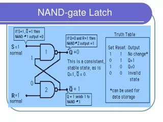
3 Input NAND GATE
Combinational Circuit Design and Simulation Using Gates. 3 Input NAND GATE. Combinational Circuit Design and Simulation Using Gates. Introduction to Digital Integrated Circuits. V CC , Power Supply Voltage Voltage supplied to integrated circuit, Nominal V CC is +5V
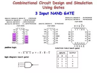

3 Input NAND GATE
E N D
Presentation Transcript
Combinational Circuit Design and Simulation Using Gates 3 Input NAND GATE
Combinational Circuit Design and Simulation Using Gates Introduction to Digital Integrated Circuits • VCC, Power Supply Voltage • Voltage supplied to integrated circuit, Nominal VCC is +5V • ICCH, Power Supply Current • Supply current required to operate IC, Output logic is “1” • ICCL, Power Supply Current • Supply current required to operate IC, Output logic is “0” • IOS, Short Circuit Output Current • Amount of current TTL output circuit can deliver into S.C • IOL, Output Current Low • Maximum output terminal sink current, Output logic is “0” • IOH, Output Current High • Maximum output terminal source current, Output logic is “1” • IIH, Current Input High • Maximum current at input terminal, Input logic is “1”
Combinational Circuit Design and Simulation Using Gates Introduction to Digital Integrated Circuits • IIL, Current Input Low • Maximum input current, Input voltage logic is “0” • VOL, Voltage Output Low • Maximum allowable output voltage, Output logic is “0” • VOH, Voltage Input High • Minimum output voltage, Output logic is “1” • VIH, Voltage Input High • Minimum logical 1 input voltage, VIH is 2 V • VIL, Voltage Input Low • Maximum logical 1 input voltage, VIL is 0.8 V • tpLH, Propagation delay time • From Output “Low” to “High” • tpHL, Propagation delay time • From Output “High” to “Low”
Introduction to Digital Integrated Circuits Signal Delay Times
Introduction to Digital Integrated Circuits 2 Input NAND(74xxx00) Parameter Values
INV 2 input NAND A.L=w’z+x’yz’ B.L=xy’z’+x’yz C.L=wx’y’z’ D.L=xy’z+w’z+x’yz’ 3 input NAND E.L=z+x’y 4 input NAND F.L=wx’y’+y’z G.L=xy’z+w’
Introduction to Digital Integrated Circuits Power Consumption Considerations • Consider power consumption and switching speed • P=(ICCave)(VCC), assume VCC=5 V • 74LS00, 74LS10, 74LS20, and 74LS04 LD00 LS10 LS20 LS04 ICCH 0.8mA 0.6mA 0.4mA 1.2mA ICCL 2.4mA 1.8mA 1.2mA 3.6mA ICCave 1.6mA 1.2mA 0.8mA 2.4mA • Total average supply current is found • ICCave = 8(1.6)+6(1.2)+2(0.8)+6(2.4)=36mA • P=5.0V(36mA)=180mW