3. Logic Gate
3. Logic Gate. 3.1 Introduction static, fully complementary CMOS psudo-nMOS, domino logic 3.2 Combinational Logic Functions combinational logic ---- specification expression logic gate networks ---- implementation area, delay, power ---- costs. literal. [Completeness]

3. Logic Gate
E N D
Presentation Transcript
3. Logic Gate • 3.1 Introduction static, fully complementary CMOS psudo-nMOS, domino logic • 3.2 Combinational Logic Functions combinational logic ---- specification expression logic gate networks ---- implementation area, delay, power ---- costs
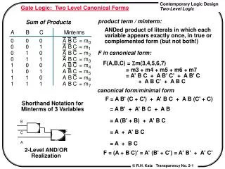
literal • [Completeness] • Function {|}=NAND function: complete • 1: a|(a|a) = a|a’ = 1 • 0: {a|(a|a}|{a|(a|a)} = 1|1 = 0. • a’: a|a = a’. • ab: (a|b)|(a|b) = ab • a+b: (a|a)|(b|b) = a’|b’=a+b • NOR function: complete • AND and OR function: not complete • [Irredundant] no literal can be removed. • redundant Ab+ab’=a
3.3 Static Complementary Gates3.3.1 Gate Structure VDD • Pullup network (pMOS) • output is connected to VDD • Pulldown network (nMOS) • Output is connected to VSS VSS
CMOS NAND • Pullup network (pMOS) • output is connected to VDD • when ab=0. VDD • Pulldown network (nMOS) • Output is connected to VSS • when ab=1. VSS
CMOS NOR • Pullup network (pMOS) • output is connected to VDD • when a+b=0. VDD • Pulldown network (nMOS) • Output is connected to VSS • when a+b=1. VSS
Static Complementary gate [a(b+c)]’ Dual graph
And Or Inverter (AOI) gate (ab+c)’
3.3.2 Basic Gate Layouts Layout of Inverter
Layout of NAND gate
Layout of NOR gate
Layout of a wide transistor by split into two sections.
3.3.3 Logic Levels VOH: minimum voltage output for logic 1. VOL: maximum voltage output for logic 0. VIH: minimum voltage input for logic 1. VIL: maximum voltage input for logic 0. VOL < VIL VOH > VIH
Minimum size transistors VOH Noise Margin NML = VIL-VOL NMH = VOH-VIH VIH VOL VIL
3.3.6 The Speed-Power Product • Speed-power product = power-delay product SP=(1/f)P=CV2
3.3.7 Layout and Parasitics Resistance parastics
3.3.8 Driving Large Loads Alpha=(Cbig/Cg)(1/n) Ttot = Nopt=
3.4 Wires and Delay3.4.1 Elmore Delay Model Delta1=r1 x (C1+---+Cn) =n rc Delta2=r2 x (C2+----+Cn) =(n-1)rc DeltaN=rn x Cn =rc total=Delta1+ ----- + DeltaN =n(n+1)/2 x rc
3.4.2 Wire Sizing Optimum-shaped wire
3.5 Switch Logic Logic 0 transfer Logic 1 transfer
3.6.2 DCVS (Differential Cascaded voltages switch logic) Logic