Download
1 / 4
40 likes | 262 Vues
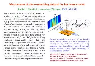
h (x,t). j (x). Mechanisms of ultra-smoothing induced by ion beam erosion Randall L. Headrick, University of Vermont, DMR-0348354.

E N D
h (x,t) j (x) Mechanisms of ultra-smoothing induced by ion beam erosionRandall L. Headrick, University of Vermont, DMR-0348354 Ion erosion of solid surfaces is known to produce a variety of surface morphologies, such as self-organized patterns composed of highly correlated arrays of dots or ripples. One effect of considerable practical importance is that of surface smoothing of nanometer features during etching or film deposition using energetic species. We have investigated pattern formation and smoothing during Ar+ ion erosion of Al2O3 and SiO2 surfaces. X-ray scattering experiments show that ion smoothing of a patterned surface is explained by a mechanism where collisions with near-surface atoms produce an effective downhill current. The results lead to predictions for the surface morphology phase diagram as a function of ion energy and incidence angle that substantially agree with experimental results. Surface morphology evolution of an initially rough surface during ion beam smoothing is investigated by real-time synchrotron x-ray scattering. An ion-collision induced downhill surface current causes rapid smoothing of nanometer scale features. H. Zhou, Y. P. Wang, L. Zhou and R. Headrick et al. Physical Review B 75, 155416 (2007) H. Zhou, L. Zhou, G. Özaydin, K. F. Ludwig Jr. and R. Headrick (submitted to Physical Review Letters)
Intensity profile evolution Surface evolution Surface Roughness Evolution During the Sputter Deposition of WSi2 Amorphous Films Randall L. Headrick, University of Vermont, DMR-0348354 Sputter deposition is a widely-used process for making thin films for an enormous range of applications. However, the detailed mechanisms of roughening and smoothing in the growth processes are not known. In this work, real-time x-ray scattering methods are employed to quantitatively investigate the surface evolution of sputter-deposited WSi2 amorphous films. The surface morphology changes from ultra-smooth to rough as the Ar background pressure in the vacuum chamber is varied. At low pressures, energetic particles can bombard the surfaces and promote smoothing, while at higher pressures the surfaces roughen rapidly. Corresponding changes in x-ray intensity profiles as a function of pressure and film thickness are used to monitor these effects. The experiments are carried out at X21-beamline at NSLS . Sketch of the real-time x-ray scattering method to study the surface morphology evolution during thin film growth by sputter deposition. The scattering pattern evolves as the film thickness and roughness spectrum change during deposition.
Structure and Carrier Mobility of Solution-Deposited Thin Film Transistors Randall L. Headrick, University of Vermont, DMR-0348354 New solution processing methods for deposition of organic semiconductor films are currently needed in order to drive research and technology in organic electronics. Direct write methods have the potential to produce large grain size films with improved electrical carrier mobility. A direct-write process using a hollow pen has been found to be effective in depositing films in narrow lines with very large grain sizes. The method has been applied to the production of Organic Field Effect Transistors (OFETs) with control of crystalline grain size, grain orientation, and field-effect carrier mobility. Transistor Channel TIPS-pentacene lines are deposited over gold source and drain contacts using a 1.0 mm pen, as shown in the inset. A polarization mode optical micrograph shows crystalline grains bridging across the 75 mm transistor channel. The scale bar represents 250 mm. R. Headrick, S. Wo, F. Sansoz, and J.E. Anthony (submitted to Applied Physics Letters)
Organic Light Emitting Diodes: a High School Outreach Project Randall L. Headrick, University of Vermont, DMR-0348354 Headrick’s group at UVM worked with a team from Stowe H.S. (Stowe, VT) during the 2006-2007 academic year on a project to study the fabrication and light output of Organic Light Emitting Diodes (OLEDs) based on polymer materials. One teacher and two students spent a week at Headrick’s lab at UVM during the month of June 2006 learning about the science and technology of OLEDs. The materials and equipment for the project were then taken to Stowe H.S., where the project was continued throughout the academic year. The team developed their own film deposition and encapsulation methods, and showed that these improvements reduced the degradation rate of the diodes. Both students started college in the Fall of 2007, and both plan to major in a science. Simple OLEDs are fabricated in several steps. Light is emitted from regions where the back contacts are attached when a small voltage is applied, and is readily visible with the room lights dimmed.