Download
1 / 8
80 likes | 354 Vues
CVD methods for manufacturing of superconducting wires. Cecilia Liss Piotr Waszkiewicz. What is superconductivity ? . Below certain temperature materials have no electric resistance. Materials also become perfect diamagnets - Meissner effect Electrons move in pairs- Cooper pairs

E N D
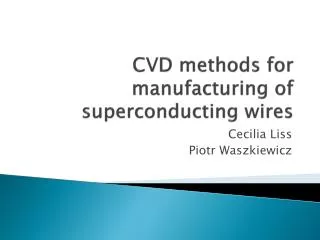
CVD methods for manufacturing of superconducting wires Cecilia Liss PiotrWaszkiewicz
What is superconductivity ? • Below certain temperature materials have no electric resistance. • Materials also become perfect diamagnets- Meissner effect • Electrons move in pairs- Cooper pairs • Superconductor is something more than perfect conductor
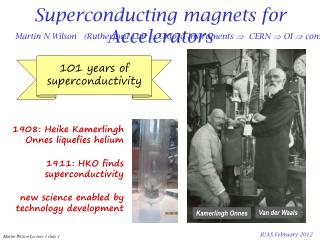
Types of superconductivity • Very low temperatures ~ 4K • Pure metals-lead, mercury, aluminum • Bulk materials • Fully described by BCS theory • First discovered in 1911- Heike KamerlinghOnnes • No magnetic penetration of material • Higher temperatures- up to ~100 K • Complex materials- YBCO, HgBa2Ca2Cu3O8+δ • Usually anisotropic behavior-layers • No theory to describe • Magnetic field penetrates in form of vortices TYPE I TYPE II
Magnetic Vortex in Type II • Magnetic field penetrates superconductor in form of magnetic vortices • Vortex- quantum portion of magnetic field • Vortices are non-superconducting regions • They are pinned to defects and form Abrikosovlattice • Vortices start to move if current density becomes to high- Ohmic resistance appears and superconductivity is destroyed.
Where nanotechnology comes in? • YBCO is superconducting only in CU-O layers • Manufacturing of superconducting cables- CVD, HPCVD, Power-In-Tube • Upgrading properties due to increase of pinning force. YBCO structure
Example- depositing YBCO and silver thin-films • Aluminum oxide substrate • Silver is deposited by CVD/laser assisted CVD as barrier layer. • YBCO is deposited in thin film also by CVD- increased current density due to thin-film properties and stronger pinning • Next layer of silver is used as contact and/or barrierlayer
Reference • Journal of Alloys and Compounds, 187 (1992) 331-349, JALCOM 324 Chemical vapor deposition of silver films for superconducting wire applications • Superconductors: Complex materials for practical Applications, Anna Palau • http://en.wikipedia.org/wiki/File:Ybco.jpg