Download
1 / 11
110 likes | 265 Vues
Light–Output Enhancement in a Nitride-Based Light-Emitting Diode With 22 Undercut Sidewalls. Presented by 李仁凱. Outline. 原理 LED 的結構圖 特性圖 LED 比較 結論 參考文獻. 原理. 使用 22° 底切側壁. 將往水平方向發射的光經由全反射,增加往上發射的機會。 θ = sin-1(nair/nGaN) ; θ: 全反射角 = sin-1(1/ 2.5) nair = 1

E N D
Light–Output Enhancement in a Nitride-Based Light-Emitting Diode With 22 Undercut Sidewalls Presented by 李仁凱
Outline • 原理 • LED的結構圖 • 特性圖 • LED比較 • 結論 • 參考文獻
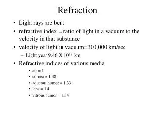
使用22°底切側壁 • 將往水平方向發射的光經由全反射,增加往上發射的機會。 θ=sin-1(nair/nGaN) ;θ:全反射角 = sin-1(1/ 2.5) nair=1 = ~ 23° nGaN=2.5
結論 • 不管是在表面做粗糙化、電流阻擋層、覆晶、垂直電極、22度底切側壁等等都是要增加LED的出光量,所以能夠增加LED的發光亮度方法非常多種、所以只要能提高出光量、高功率的LED就能的亮度就能再往上提升。
參考文獻 • [1] S. Nakamura, M. Senoh, N. Iwasa, and S. Nagahama, “High-brightness InGaN blue, green, and yellow light-emitting diodes with quantum well structures,” Jpn. J. Appl. Phys., vol. 34, pp. L797–L799, 1995. • [2] S. Nakamura, T. Mukai, and M. Senoh, “Candela-class high-brightness InGaN/AlGaN double-heterostructure blue-light-emitting diodes,”Appl. Phys. Lett., vol. 64, pp. 1687–1689, 1994. • [3] S. Nakamura, M. Senoh, S. Nagahama, N. Iwasa, T. Yamada, T.Matsushita, Y. Sugimoto, and H. Kiyoku, “Room-temperature continuous-wave operation of InGaN multi-quantum-well-structure laserdiodes with a long lifetime,” Appl. Phys. Lett., vol. 70, pp. 868–870,1997. • [4] T. Mukai and S. Nakamura, “Ultraviolet InGaN and GaN singlequantum-well-structure light-emitting diodes grown on epitaxially laterally overgrown GaN substrates,” Jpn. J. Appl. Phys., vol. 38, pp.5735–5739, 1999. • [5] C. Huh, K. S. Lee, E. J. Kang, and S. J. Park, “Improved light-output and electrical performance of InGaN-based light-emitting diode by microroughening of the p-GaN surface,” J. Appl. Phys., vol. 93, pp. 9383–9385,2003. • [6] J. J. Wierer, D. A. Steigerwald, M. R. Krames, J. J. O’shea, M. J. Ludowise,G. Christenson, Y. C. Shen, C. Lowery, P. S. Martin, S.Subramanya,W. Gotz, N. F. Gardner, R. S. Kern, and S. A. Stockman, “Highpower AlGaInN flip-chip light-emitting diodes,” Appl. Phys. Lett., vol.78, pp. 3379–3381, 2001. • [7] S. X. Jin, J. Li, J. Y. Lin, and H. X. Jiang, “InGaN’GaN quantum well interconnected microdisk light emitting diodes,” Appl. Phys. Lett., vol.77, pp. 3236–3238, 2000. • [8] T. N. Oder, J. Shakya, J. Y. Lin, and H. X. Jiang, “III-nitride photonic crystals,” Appl. Phys. Lett., vol. 83, pp. 1231–1233, 2003. • [9] T. N. Oder, K. H. Kim, J. Y. Lin, and H. X. Jiang, “III-nitride blue and ultraviolet photonic crystal light emitting diodes,” Appl. Phys. Lett., vol.84, pp. 466–468, 2004. • [10] H.W. Choi, M. D. Dawson, P. R. Edwards, and R.W. Martin, “High extraction efficiency InGaN micro-ring light-emitting diodes,” Appl. Phys. Lett., vol. 83, pp. 4483–4485, 2003. • [11] T. Fujii, Y. Gao, R. Sharma, E. L. Hu, S. P. DenBaars, and S. Nakamura,“Increase in the extraction efficiency of GaN-based light-emitting diodes via surface roughening,” Appl. Phys. Lett., vol. 84, pp. 855–857, 2004. • [12] W. Schmid, F. Eberhard, M. Schauler, M. Grabherr, R. King, M. Miller,E. Deichsel, G. Stareev, U. Martin, R. Jaeger, J. Joos, R. Michalzik, and K. J. Ebeling, “Infrared light-emitting diodes with lateral outcoupling taper for high extraction efficiency,” Proc. SPIE, vol. 3621, pp. 198–205,1999. • [13] S. J. Lee and S. W. Song, “Efficiency improvement in light-emitting diodes based on geometrically deformed chips,” Proc. SPIE, vol. 3621,pp. 237–248, 1999. • [14] M. R. Krames, M. Ochiai-Holcomb, G. E. Hofler, C. Carter-Coman, E.I. Chen, I.-H. Tan, P. Grillot, N. Gardner, H. C. Chui, J.-W. Huang,S. A. Stockman, F. A. Kish, M. G. Craford, T. S. Tan, C. P. Kocot, M. Hueschen, J. Posselt, B. Loh, G. Sasser, and D. Collins, “High-power truncated-inverted-pyramid (Al Ga ) In P/GaP light-emitting diodes exhibiting >50% external quantum efficiency,” Appl. Phys. Lett., vol. 75, pp. 2365–2367, 1999. • [15] D. Eisert and V. Harle, “Simulations in the development process of GaNbased LEDs and laser diodes,” in Int. Conf. Numerical Simulation of Semiconductor Optoelectronic Devices, 2002, Session 3: Photonic Devices,invited paper. • [16] C. S. Chang, S. J. Chang, Y. K. Su, C. T. Lee, Y. C. Lin, W. C. Lai, S.C. Shei, J. C. Ke, and H. M. Lo, “Nitride-based LEDs with textured side walls,” IEEE Photon. Technol. Lett., vol. 16, no. 3, pp. 750–752, Mar.2004. • [17] C. C. Kao, H. W. Huang, H. C. Kuo, J. T. Chu, C. C. Yu, C. F. Lin, and S. C. Wang, “Control of the GaN Etching Profile in Cl /Ar Inductively Coupled Plasma Reactive Ion Etching,” Mater. Sci. Eng. B, submittedfor publication.