Gain
Drift (HV 2). Gaz (ex: Ar + 5% isobutane). Conversion gap: 1 mm to m. E ~ 1kV/cm. e -. Mesh (HV 1). Amplification gap ~ 100 m m. E ~ 50 kV/cm. Strips or pads. Ionizing particle. Pad readout. Le pain. UV. La tartine. The sandwich. The pizza. UV insolator. Le bulk !!!.

Gain
E N D
Presentation Transcript
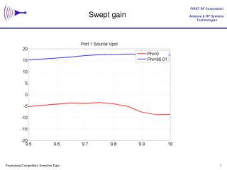
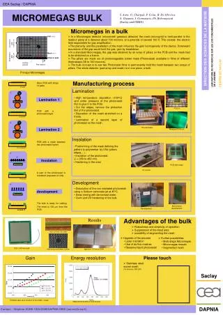
Drift (HV 2) Gaz (ex: Ar + 5% isobutane) Conversion gap: 1 mm to m E ~ 1kV/cm e- Mesh (HV 1) Amplification gap ~ 100 mm E ~ 50 kV/cm Strips or pads Ionizing particle Pad readout Le pain UV La tartine The sandwich The pizza UV insolator Le bulk !!! Development Saclay DAPNIA CEA Saclay / DAPNIA MICROMEGAS BULK S. Aune, G. Charpak, P. Colas, R. De Oliveira, A. Giganon, I. Giomataris,Ph. Rebourgeard (Saclay and CERN) Micromegas in a bulk • In a Micromegas detector (micromesh gaseous detector) the mesh (microgrid) is held parallel to the readout plane at a distance about 100 microns, at a potential of several 100 V. This creates the electric field responsible for gas amplification. • The planarity and the parallelism of the mesh influence the gain homogeneity of the device. Downward excursions of the gap would limit the gas gain by breakdown. • In a standard Micromegas, the gap was obtained by an array of pillars on the PCB and the mesh had to be stretched on a frame. • The pillars are made out of photoimageable solder mask (Photoresist) available in films of different thicknesses (38 to 100 microns). • The bulk concept is to use two Photoresist films to permanently hold the mesh between two arrays of pillars. The whole detector (pad array and mesh) is in one piece, a bulk. LABORATOIRE DE RECHERCHE SUR LES LOIS FONDAMENTALES DE L’UNIVERS CENTRE DE SACLAY DIRECTION DES SCIENCES DE LA MATIERE Principe Micromegas Manufacturing process Bare PCB with strips or pads Lamination 1 • High temperature deposition (100°C) and under pressure of the photoresist film to glue it to the PCB. • Cut the edges, remove the protection film of the photoresist. • Deposition of the mesh stretched on a frame. • Lamination of a second layer of photoresist on the mesh. Lamination 1 PCB in PCB with a photoresist layer 2 The laminator Lamination 2 Wrapped PCB out Insolation PCB with a mesh between two photoresist layers • Positionning of the mask defining the pattern to polymerise by UVs (pillars, edges,...). • Insolation of the photoresist. • (l = 350 to 450 nm). • Hardening in the oven 3 Insolation PCB with mask A part of the photoresist is insolated (exposed to UVs) Development 4 • Dissolution of the non insolated photoresist using a Sodium carbonate jet at 40°C. • Deep rinsing with de-ionised water. • Oven and UV hardening of the bulk. development The bulk is ready for cabling. The mesh is 100 mmfrom the PCB. Bulk before development Results Advantages of the bulk • Robustness and simplicity of operation • Suppression of the dead area • possibility of segmenting the mesh Laser cut mesh (70m wide) • Upgrade of the process • Laser insolation • Use of de fine meshes • Resistive liquid photoresist • Further possibilities • Multi-stage Micromegas • Micromegas mosaïc • Segmented mesh 120 x 140 mm bulk Mesh prisonned between 2 pillars Application: T2K test at CERN Gain Energy resolution Please touch • Stainless steel woven mesh (19 microns, 500 LPI) Detector gain as a function of the mesh voltage Mesurements with a Fe55 source Contact : Stéphan AUNE CEA/DSM/DAPNIA/SEDI (saune@cea.fr)