Download
1 / 25
290 likes | 483 Vues
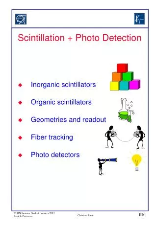
Scintillation + Photo Detection Inorganic scintillators Organic scintillators Geometries and readout Fiber tracking Photo detectors. Scintillation Two material types : Inorganic and organic scintillators. Scintillation. Energy deposition by ionizing particle

E N D
Scintillation + Photo Detection Inorganic scintillators Organic scintillators Geometries and readout Fiber tracking Photo detectors Christian Joram
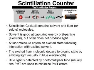
Scintillation Two material types: Inorganic and organic scintillators Scintillation Energy deposition by ionizing particle production of scintillation light (luminescense) Scintillators are multi purpose detectors calorimetry time of flight measurement tracking detector (fibers) trigger counter veto counter ….. high light output lower light output but slow but fast Christian Joram
Three different scintillation mechanisms: 1a. Inorganic crystalline scintillators (NaI, CsI, BaF2...) Inorganic scintillators often 2 time constants: • fast recombination (ns-ms) from activation centre • delayed recombination due to trapping ( 100 ms) Due to the high density and high Z inorganic scintillator are well suited for detection of charged particles, but also of g. Christian Joram
Light output of inorganic crystals shows strong temperature dependence 1b. Liquid noble gases (LAr, LXe, LKr) Inorganic scintillators (From Harshaw catalog) BGO PbWO4 also here one finds 2 time constants: few ns and 100-1000 ns, but same wavelength. Christian Joram
Properties of some inorganic scintillators Inorganic scintillators Photons/MeV 4 104 1.1 104 1.4104 6.5 103 2 103 2.8 103 PbWO4 8.28 1.82 440, 530 0.01 100 LAr 1.4 1.295) 120-170 0.005 / 0.860 LKr 2.41 1.405) 120-170 0.002 / 0.085 LXe 3.06 1.605) 120-170 0.003 / 0.022 4 104 5) at 170 nm Christian Joram
Inorganic scintillators PbWO4 ingot and final polished CMS ECAL scintillator crystal from Bogoroditsk Techno-Chemical Plant (Russia). Christian Joram
2. Organic scintillators: Monocrystals or liquids or plastic solutions Monocrystals: naphtalene, anthracene, p-terphenyl…. Liquid and plastic scintillators They consist normally of a solvent + secondary (and tertiary) fluors as wavelength shifters. Fast energy transfer via non-radiative dipole-dipole interactions (Förster transfer). shift emission to longer wavelengths longer absorption length and efficient read-out device Organic scintillators Scintillation is based on the 2 p electrons of the C-C bonds. Emitted light is in the UV range. Christian Joram
Some widely used solvents and solutes After mixing the components together plastic scintillators are produced by a complex polymerization method. Some inorganic scintillators are dissolved in PMMA and polymerized (plexiglas). Organic scintillators (backup) Schematic representation of wave length shifting principle (C. Zorn,Instrumentation In High Energy Physics, World Scientific,1992) Christian Joram
Organic scintillators yield/ NaI 0.5 Organic scintillators have low Z (H,C). Low g detection efficiency (practically only Compton effect). But high neutron detection efficiency via (n,p) reactions. Christian Joram
Scintillator readout Readout has to be adapted to geometry and emission spectrum of scintillator. Geometrical adaptation: Light guides: transfer by total internal reflection (+outer reflector) wavelength shifter (WLS) bars Scintillator readout “fish tail” adiabatic Christian Joram
Optical fibers minimize ncladding. Ideal: air (n=1), but impossible due to surface imperfections Scintillator readout light transport by total internal reflection in one direction multi-clad fibres for improved aperture and absorption length: l>10 m for visible light Christian Joram
Scintillating fiber tracking Scintillating fiber tracking • Scintillating plastic fibers • Capillary fibers, filled with liquid scintillator Planar geometries (end cap) Circular geometries (barrel) a) axial b) circumferential c) helical (R.C. Ruchti, Annu. Rev. Nucl. Sci. 1996, 46,281) • High geometrical flexibility • Fine granularity • Low mass • Fast response (ns) (if fast read out) first level trigger Christian Joram
Scintillating fiber tracking Charged particle passing through a stack of scintillating fibers (diam. 1mm) UA2 (?) Hexagonal fibers with double cladding. Only central fiber illuminated. Low cross talk ! 3.4 mm 60 mm (H. Leutz, NIM A 364 (1995) 422) Christian Joram
Photo Detectors Photo Detectors Purpose: Convert light into detectable electronics signal Principle: Use Photoelectric Effect to convert photons to photoelectrons • standard requirement • high sensitivity, usually expressed as • quantum efficiencyQ.E. = Np.e./ Nphotons • Main types of photodetetcors • gas based devices (see RICH detectors) • vacuum based devices • solid state detectors Threshold of some photosensitive material GaAs ... UV visible multialkali TMAE,CsI bialkali TEA E (eV) 12.3 4.9 3.1 2.24 1.76 100 250 400 550 700 l (nm) Christian Joram
Photo Detectors Photoelectric effect in photocathodes • 3-step process • photo ionization of molecule • Electron propagation through cathode • escape of electron back into the vacuum Semitransparent photocathode Opaque photocathode g g glass PC substrate e- e- PC Most photocathodes are semiconductors: band model: Photon energy has to be sufficient to bridge the band gap Eg, but also to overcome the electron affinity EA, so that the electron can be released into the vacuum. Christian Joram
Quantum efficiencies of typical photo cathodes Photo Detectors Q.E. Bialkali SbK2Cs SbRbCs Multialkali SbNa2KCs Solar blind CsTe (cut by quartz window) (Philips Photonic) Transmission of various PM windows NaF, MgF2, LiF, CaF2 Christian Joram
Photo Multiplier Tube (PMT) Vacuum Based Photo Detectors photon e- (Philips Photonic) main phenomena: • photo emission from photo cathode. • secondary emission from dynodes. dynode gain g=3-50 (f(E)) total gain 10 dynodes with g=4 M = 410 106 Christian Joram
Energy resolution of PMT’s Vacuum Based Photo Detectors The energy resolution is determined mainly by the fluctuation of the number of secondary electrons emitted from the dynodes. Poisson distribution: Relative fluctuation: Fluctuations biggest, when small ! First dynode ! GaP(Cs) Negative electron affinity (NEA) ! (Philips Photonic) (Philips Photonic) Single photons. Pulse height spectrum of a PMT with Cu-Be dynodes. Pulse height spectrum of a PMT with NEA dynodes. 1 p.e. counts counts (Philips Photonic) 1 p.e. 2 p.e. 3 p.e. noise (H. Houtermanns, NIM 112 (1973) 121) Pulse height Pulse height Christian Joram
Dynode configurations Vacuum Based Photo Detectors traditional New ‘micro-machined’ structures (Philips Photonics) position sensitive PMT’s PM’s are in general very sensitive to B-fields, even to earth field (30-60 mT). m-metal shielding required. Christian Joram
Vacuum Based Photo Detectors Multi Anode PMT example: Hamamatsu R5900 series. Up to 8x8 channels. Size: 28x28 mm2. Active area 18x18 mm2 (41%). Bialkali PC: Q.E. = 20% at lmax = 400 nm. Gain 106. Gain uniformity and cross-talk used to be problematic, but recently much improved. Very recent development: Flat Panel PMT (Hamamatsu ) Excellent surface coverage (>90%) 8 x 8 channels (4 x 4 mm2 / channel) Bialkali PC, eQ 20% 50 mm Christian Joram
Hybrid photo diodes (HPD) Vacuum Based Photo Detectors photo cathode + p.e. acceleration + silicon det. (pixel, strip, pads) Photo cathode like in PMT, DV 10-20 kV (for DV =20 kV) Commercial HPD (DEP PP0270K) with slow electronic (2ms shaping time) (C.P. Datema et al. NIM A 387(1997) 100 Single photon detection with high resolution Poisson statistics with =5000 ! Background from electron backscattering from silicon surface Christian Joram
Cherenkov ring imaging with HPD’s Vacuum Based Photo Detectors (CERN) 2048 pads Pad HPD, Ø127 mm, fountain focused test beam data, 1 HPD (LHCb - DEP) 3 x 61 pixels Pixel-HPD, 80mm Ø cross-focused test beam data, 3 HPDs Christian Joram
Photo diodes Solid State Photo Detectors p h e P(I)N type n = i (intrinsic) n+ p layer must be very thin (<1 mm), as visible light is rapidly absorbed by silicon. High Q.E. (80% at l 700nm), but no gain: G = 1. Can’t be used for single photon detection, but suitable for readout of scintillators. Even better… • Avalanche Photo diodes (APD) High reverse bias voltage 100-200V. High internal field avalanche multiplication. G 100(0) E p h e drift p n avalanche Christian Joram
Visible Light Photo Counter VLPC Photo Detectors (backup) Gain Drift Substrate Hole drifts towards highly doped drift region and ionizes a donor atom free electron. Multiplication by ionization of further neutral donor atoms. Region Region Intrinsic Spacer Region Region • e • e • h Photon • + • - Si:As impurity band conduction avalanche diode 1.0 0.8 0.6 0.4 0.2 0.0 Q.E. • Operation at low bias voltage (7V) • High IR sensitivity Device requires cooling to LHe temperature. • Q.E. 70% around 500 nm. • Gain up to 50.000 ! VLPC bialkali (ST) GaAs (opaque) Multialkali (ST) 300 400 500 600 700 800 900 1000 l (nm) Christian Joram
no light pedestal noise events with light events 0 1 2 3 4 5 ADC counts (a.u.) Photo Detectors (backup) High gain real photon counting as in HPD Fermilab: D0 (D zero) fiber tracker (72.000 channels) 8 pixels per chip (vapour phase epitaxial growth) Ø1 mm Christian Joram