CLIC DB injector study
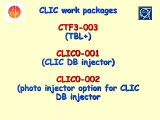
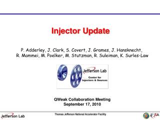
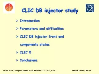
CLIC DB injector study. Introduction Parameters and difficulties CLIC DB injector front end components status CLIC 0 Conclusions. CLIC DB injector schematics. Solenoids. Thermionic gun. Buncher. SHB. Prebuncher. Accelerating cavity. 6 M e V. Slit. 26 M e V. 53 M e V.

CLIC DB injector study
E N D
Presentation Transcript
CLIC DB injector study • Introduction • Parameters and difficulties • CLIC DB injector front end components status • CLIC 0 • Conclusions
CLIC DB injector schematics Solenoids Thermionic gun Buncher SHB Prebuncher Accelerating cavity 6 MeV Slit 26 MeV 53 MeV Documented in the CDR; a scaled version of CTF3 Simona Bettoni, Alessandro Vivoli
Sub Harmonic Bunchers (SHBs) even buckets odd buckets • RF deflector n0 / 2 Gap creation and combination Main challenge of SHBs: Fast 180° phase flipping capability, simulation indicate < 18 ns switching time needed Phase coding Sub-harmonic bunching n0 / 2 Modulator-klystrons, 1 GHz, 15 MW IOTs, 500 MHz Diagnostics 180 phase switch Acceleration n0 SHB 1-2-3 Gun PB Buncher Acc. Structures ~ 12 MeV ~ 140 keV Deflection n0 / 2
Simulation results Longitudinal phase space after sub-harmonic bunching Same total gap-voltage but fewer cells (2 instead of 6) 35-39 KV needed
Simulation results • Specifications can be fulfilled but still high satellite population and high losses in cleaning chicane • Some ideas to improve the satellites and total losses • Beam loading and wake field effects to be studied • Some inconsistencies due to a lack of realistic rf-parameters (simulations have to be redone with new parameters)
CLIC DB front end, Post CDR Project Modulator-klystrons, 1 GHz, 15 MW IOTs, 500 MHz Diagnostics SHB 1-2-3 Gun PB Buncher Acc. Structures ~ 3 MeV ~ 12 MeV ~ 140 keV Gun, sub-harmonic bunching, bunching, three accelerating structures, 5 long pulse klystrons and modulators, diagnostics
What do we plan to do until 2016 Optimistic and rough planning Create a gun test facility to test the source and a high power test stand to test the klystron, modulator and rf structures
Gun options CTF3 type gridded gun with a HV modulator, Modulator stability, grid survival, several SHB needed, can be purchased Modulated anode gun, needs new design and simulation, Can’t be bought of the shelf, not sure if modulation fulfills requirements 3. RF modulated grid, IOT-type gun, very attractive but needs tests and simulation, dark current issue, emittance ?, reliability, can be purchased, no SHB, no satellites, likely R&D needed RF Modulate classical gun, typical pulse length 1 ns, could have very low satellites, can this deliver enough current, space charge problems
Sub-harmonic bunching system Status: RF design existing, ready to start mechanical design and launch prototype or cold model Power source: 500 MHz, ~100 kW, wide band (70 MHz) sources needed for fast phase switching. Started to discuss with industry. Candidates: IOT, frequency and power available, bandwidth to be seen tests are planned with an 800 MHz IOT for SPS Solid state amplifier, bandwidth, power, cost ? RF design of 1 GHz pre-buncher and travelling wave buncher existing
Magnetic coupling TW structure For the known gap voltage and filling time our goal is to increase R/Q to reduce the input power. τ=10ns V=36.5 KV lc rc θc r1 t/2 θ1 g rn rb l
Phase flipping simulation with beam – 10 ns Excitation signal from port 1 with 80 KW peak power. port 2 port 1 Beam Entrance Continues beam with 6A current
Phase flipping simulation with beam – 10 ns Excitation signal – port 1 Output signal – port 2 ≈ 12 ns ≈ 44 ns Output signal – port 1
Phase flipping simulation with beam – 10 ns About 5 bunches will be missed in comparison with about 120 bunches in each sub-pulse.
DB-accelerator structure RF-design existing, next steps: mechanical design and prototype Input and output coupler design finished Correct match, input reflection < 30 dB. (red and green: two different geometries; red is final) Rolf Wegener
DB-accelerator structure Parameters: f = 999.5 MHz Pin= 15 MW RB= 49 mm N= 19 cells OD= 300 mm L= 2.4 m Tfill = 245 ns hRF-Beam= 97.5 % Rolf Wegener
RF power sources 1 GHz high efficiency klystron Development and Purchasing strategy: Launch tender to develop and purchase high efficiency klystrons in industry. Aim for multiple vendors. Klystrons could arrive from 2015 in line with modulator development Plan to hold a workshop on high efficiency klystrons and modulators in spring 2013 (EuCard2 network on high efficiency rf sources). Seeking collaborations for this topic !
CLIC studies & klystron modulators specs Pulse efficiency definition Approach: Develop and explore with collaboration partners technologies to meet the ultimate specification for CLIC with the goal to have two working prototypes in 2015-2016. First collaboration with ETH Zürich started, prototype in 2015 ~300MW required for kly. mod. CLIC Drive Beam klystron modulators R&D strategy
Demonstration goals for the injector front end • Demonstrate rf system at full pulse length and beam loading High efficiency klystron High efficiency and stable modulator Full loaded accelerating structure (validate technology) • Demonstrate beam quality and stability requirements for long pulse Current stability 0.1% Beam phase stabilityEmittance and energy and position jitter • Demonstrate electron source and phase coding Life time, reliability, routine operation • Demonstrate diagnostics suitable for long pulse and machine protection • DB Injector suitable for CLIC zero and CLIC
Photo injector option • Advantages • No satellites or tails, phase coding on the laser side • No or less bunching needed, possibly better emittance • Flexible time structure (single bunches) • Concerns • Cathode lifetime • Challenging laser, peak and average power • Intensity stability • Maintenance and operation • Very little resource available for time being
Introduction to 20 % of the CLIC Drive Beam and 10 % of a CLIC decelerator C CALIFES type injector 0.25 GeV, 1.2 A zero TBA 6.5 GeV, 1.2 A 0.2 GeV, 101 A DB Turn around0.48 GeV, 101 A CR1 DBA 0.48 GeV, 4.2 A DL CR2 Compression2 x 3 x 4 100 m H. Braun, CLIC 2008 Workshop
Motivation for CLICzero • Demonstrate nominal drive beam parameters (except the energy) Full combination scheme to 100 A, full pulse length in injector • Realizetwo beam acceleration with nominal hardware for a significant length (~100 m) • Drives industrialization, needed to be ready for CLIC Significant size series production of cost and performance driving hardware (46 two beam modules, 276 x-band structures, 138 PETS, 140 L-band klystrons, modulators and structures) • Most hardware reusable for CLIC • Could be a beam driven processing facility for the x-band structures • Drawbacks: • Expensive • Beam dynamics for combination might be more difficult due to lower energy • Does not address sufficiently emittance preservation and luminosity issues
Conclusions • Unusual parameter space for an injector • Rough conceptual design for the injector exists, now we have to get really started • Plans for purchasing the key hardware items have been developed and need to be followed up now • We seeking collaborationsfor this work, anybody interested ?
Klystron specifications TH1802, ILC MBK klystron CLIC DB klystron design goal, ~ 150kV voltage was assumed for time being
Features of CLICzero • Nominal CLIC DB injector • Nominal DB rf system (Klystron, Modulator, accelerating structure) • Nominal 100 A drive beam (6 ms) • 20 % drive beam energy • Nominal Delay Loop and Combiner Rings (1/5 of the energy) • Drive beam pulse shaping can be studied • DB turn around to study phase feed forward • 46 nominal two beam modules (type 1; ~ 100 m) • 10% of a decelerator (last 10 % most difficult) • 6.25 GeV electron beam, 1.2 A • Nominal beam loading
CLIC studies & klystron modulators specs Technology challenges Machine availability With more than 1600 modulators, reliability, modularity & redundancy must be optimized for maximum accelerator availability Pulse to pulse reproducibility: 10 to 100ppm • Modulator topology selection considering: • Efficiency maximization (max. power limited) • Reproducibility • Constant power consumption • Satisfactory accelerator availability Modulator and voltage measurement reproducibility never achieved before! AC power quality optimization More than 1600 modulators pulsing synchronously! Utility grid power fluctuation minimized (~1%) – tough charger design Need for a global approach! Different solutions must be explored (transformer based, fully solid state, HV & LV solutions) CLIC Drive Beam klystron modulators R&D strategy
What is needed to get ready for CLICzero • Prototyping and small series production of major hardware DB-klystron, DB acc-structure, Modulator, Diagnostics, two beam modules • DB injector design and demonstration (Source, phase coding, stability) includes prototyping of DB rf system • Technical design of the DB linac • Technical design of the beam combination complex (delay loop, combiner rings) • Technical design of the turn around loop • Technical design of the probe beam injector • Technical design and prototyping of the two beam modules (acc-structure, PETS, diagnostics, Quads, stabilization and alignment) • Study and prepare location and implementation (tunnel, building) • …..
Four cells structure with waveguide couplers In this design for the first SHB about 73 kW peak power is needed for 10ns filling time and 36.5 KV gap voltage.
Phase flipping simulation – 10 ns Excitation signal – port 1 Output signal – port 2 ≈ 14 ns ≈ 34 ns Output signal – port 1 CLIC Collaboration Working meeting- 2012
Phase flipping simulation – 26 ns Excitation signal – port 1 Output signal – port 2 ≈ 20 ns Output signal – port 1 ≈ 40 ns CLIC Collaboration Working meeting- 2012
Borrowed from Oleksiy Kononenko Phase flipping- how fast? In the normal case the time interval between phase switching is constant (243.7 ns). In the Oleksiy model these intervals are not constant to have better energy dispersion at the end of main beam linac. It also give us an idea that how much the minimum phase flipping should be. The result shows us it should be less than 18ns. In my design I use 10ns similar to CTF3 SHBs. CLIC Collaboration Working meeting- 2012
Parameter for optimization Travelling Wave Structure For the known gap voltage and filling time our goal is to increase R/Q to reduce the input power. R : Effective shunt impedance R’: Effective shunt impedance per length Q : Unloaded quality factor P: Source power V : Gap voltage W’ : Stored energy per length L: Structure length vg : Group velocity n : Cell numbers τ=10ns V=36.5 KV Pd : Power disappears on surface. β : Coupling coefficient Qe = ωτ : External quality factor τ : Filling time CLIC Collaboration Working meeting- 2012
Electron source options Some simple considerations • CTF3: 1.6 ms, 9.6mC per pulse • 1 % droop specs • 7 nF, ~70 J stored energy • CLIC: 140 ms, 700 mC per pulse • 0.1 % droop specs • 5 mF, ~50 kJ stored energygridded cathode might not survive • CTF3 gun concept might be not scalable for CLIC