Digital Signal Processing
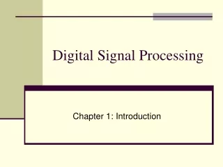
Digital Signal Processing. Analog signal (time varying, continuous). Incoming samples. Vref. Analog-to-Digital Converter (ADC). 0x030, 0x4A, 0x12, 0xAF, etc. 0. Time. Vref. Digital-to-Analog Converter (DAC). 0x0B3, 0x23, 0xCF, 0x78, etc. Processor performs computation. new waveform.

Digital Signal Processing
E N D
Presentation Transcript
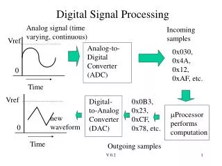
Digital Signal Processing Analog signal (time varying, continuous) Incoming samples Vref Analog-to-Digital Converter (ADC) 0x030, 0x4A, 0x12, 0xAF, etc. 0 Time Vref Digital-to-Analog Converter (DAC) 0x0B3, 0x23, 0xCF, 0x78, etc. Processorperforms computation new waveform 0 Time Outgoing samples V 0.2
Applications • Audio • Speech recognition • special effects (reverb, noise cancellation, etc) • Video • Filtering • Special effects • Compression • Data logging V 0.2
Vocabulary • ADC (Analog-to-Digital Converter) – converts an analog signal (voltage/current) to a digital value • DAC (Digital-to-Analog Converter) – converts a digital value to an analog value (voltage/current) • Sample period – for ADC, time between each conversion • Typically, samples are taken at a fixed rate • Vref (Reference Voltage) – analog signal varies between 0 and Vref, or between +/- Vref • Resolution – number of bits used for conversion (8 bits, 10 bits, 12 bits, 16 bits, etc). • Conversion Time – the time it takes for a analog-to-digital conversion V 0.2
Digital-to-Analog Conversion For a particular binary code, output a voltage between 0 and Vref Vref D[7:0] Vout DAC Assume a DAC that uses an unsigned binary input code, with 0 < Vout < Vref. Then D= 0000 0000 Vout = 0VD= 0000 0001 Vout = Vref(1/256 ) (one LSB)D = 0000 0010 Vout = Vref(2/256)...D = 1111 1111 Vout = Vref(255/256) (full scale) V 0.2
DAC Output Plot Vout Output signal increases in 1 LSB increments. 4/256 Vref 3/256 Vref 2/256 Vref 1/256 Vref 0 1 2 3 Input code V 0.2
Typical DAC Output From http://www.allaboutcircuits.com V 0.2
DAC Architecture Operational Amplifier can be used to sum voltages. From http://www.allaboutcircuits.com V 0.2
DAC Architecture (cont) Note ratios of resistors This is a binary code From http://www.allaboutcircuits.com V 0.2
DAC Architecture (cont) A 3-bit DAC, called an R/2NR DAC. Resistors are scaled by powers of 2 (this is hard to do in practice). From http://www.allaboutcircuits.com V 0.2
Another View Resistance values are still R, 2R, 4R From http://www.allaboutcircuits.com V 0.2
R/2R DAC Via circuit analysis, can prove this is an equivalent circuit. Now only need resistances of R, 2R – this is easy to do. This is the most common DAC architecture. From http://www.allaboutcircuits.com V 0.2
Commercial DACs • Either voltage or current DACs • Current DACs require an external operational amplifier to convert to voltage • Precision up to 16-bits • Key timing parameter is settling time - amount of time it takes to produce a stable output voltage once the input code has changed • We will use an 8-bit voltage DAC with an I2C interface from Maxim semiconductor V 0.2
DAC Application Phosper Vertical Deflection Cathode R Red DAC Electron Beams (Red, Green Blue) Green 8 G DAC 8 Blue B DAC 8 Grid Horizontal Deflection High speed video DACs produce RGB signals for color CRT V 0.2
A 1-bit ADC analog signal Vdd Vref Vin + R Vout=Vdd is Vin > Vref/2 Vref/2 - Vout=0 if Vin < Vref/2 R digital signal comparator V 0.2
+ + + - - - A 2-bit ADC R Vin A 3/4Vref A B C D1 D0-------------0 0 0 0 00 0 1 0 10 1 1 1 01 1 1 1 1 (other codesdon’t cares) R D[1:0] Vin B 1/2Vref R C Vin 1/4Vref R Encoding logic V 0.2
ADC Architectures • The previous architectures are called Flash ADCs • Fastest possible conversion time • Requires the most transistors of any architecture • N-bit converter requires 2N-1 comparators. • Commercially available flash converters up to 12 bits. • Conversion done in one clock cycle • Successive approximation ADCs • Use only one comparator • Take one clock cycle per bit • High precision (16-bit converters are available) V 0.2
Successive Approximation ADC First, set DAC to produce Vref/2. Output of Comparator is Q[N-1] (MSB) If MSB =1 , then Vin between Vref and Vref/2, so set DAC to produce ¾ Vref. If MSB=0, then Vin between Vref/2 and 0, so set DAC to ½ Vref. Output of comparator is now Q[N-2]. Do this for each bit. Takes N cycles. Output is Q[N]. From http://www.allaboutcircuits.com V 0.2
Commercial ADCs • Key timing parameter is conversion time – how long does it take to produce a digital output once a conversion is started • Up to 16-bit ADCs available • Separated into fast/medium/low speed families • Serial interfaces common on medium/low speed ADCs • For high-precision ADCs, challenge is keeping system noise from affecting conversion • Assume a 16-bit DAC, and a 4.1V reference, then 1 LSB = 4.1/216 = 62 V. V 0.2
ADC, DAC Equations ADC: Vin = input voltage, Vref = reference voltageN = number of bits of precision Vref output code Vin/ Vref * 2N = output_codeoutput_code/ 2N * Vref = Vin 1 LSB = Vref/2N ADC Vin N DAC: Vout = output voltage, Vref = reference voltage, N = number of bits of precision Vref Vout input code Vout/ Vref * 2N = input_codeinput_code/ 2N * Vref = Vout 1 LSB = Vref/2N DAC N V 0.2
Sample ADC Computations If Vref = 5V, and the 10-bit A/D output code is 0x12A, what is the ADC input voltage? output_code/2N * Vref = (0x12A)/210 * 5 V = 298/1024 * 5 V = 1.46 V (Vin) If Vref = 5V, and the upper 8 bits of the A/D output code is 0xA9, what is the ADC input voltage? output_code/2N * Vref = (0xA9)/28 * 5 V = 169/256 * 5 V = 3.3 V (Vin) If Vref = 4V, and the A/D input voltage is 2.35 V, what is the ADC output code, upper 8-bits? Vin/ Vref * 2N = 2.35 V/ 4 V * 28 = .5875 * 256 = 150.4 = 150 = 0x96 V 0.2
Sample DAC Computations If Vref = 5V, and the 8-bit input code is is 0x8A, what is the DAC output voltage? input_code/2N * Vref = (0x8A)/28 * 5 V = 138/256 * 5 V = 2.70 V (Vout) If Vref = 4V, and the DAC output voltage is 1.25 V, what is the 8-bit input code? Vout/ Vref * 2N = 1.25 V/4 V * 28 = 0.3125 * 256 = 80 = 0x50 (input_code) V 0.2
PIC18 A/D • PIC18F242 has onboard A/D • Successive approximation • 10 bit resolution • Reference voltage can be Vdd or separate voltage • Multiple input (more than one input channel) • Time per bit(Tad) for conversion is either 2Tosc, 8Tosc, or 32 Tosc, where Tad cannot be less than 1.6 us (Tosc = 1/Fosc) • Total conversion time is 10* Tad +Taq (acquisition) • Taq is approximately 20 us; acquisition time is the amount of time input capacitor requires to charge up to input voltage. • So a 20 Mhz Fosc, Tosc = .05 us, so 32Tosc = 1.6 us; conversion time = 10*1.6 us + 20 us = 36 us. V 0.2
Input Pins Analog input channels (AN0,AN1, AN4) Can be analog input channels or Vref+/Vref- V 0.2
A/D Block Diagram Channel select analog mux. Vref+/Vref- select V 0.2
Acquisition Time Acquisition time is the time required for the analog input voltage to be sampled by the input capacitor. The sampling switch is CLOSED during this time. When the conversion begins, the sampling switch is OPENED and the input capacitor holds the input voltage while the conversion is done. This process is also called sample and hold. V 0.2
Voltage References Stability of voltage reference is critical for high precision conversions. We will use Vdd as our voltage reference for convenience, but will be throwing away at least two bits of precision due to Vdd fluctations. Example Commercial voltage reference: 2.048v, 2.5v , 3v, 3.3v, 4.096v, 5v (Maxim 6029) Key parameter for a voltage is stability over temperature operating range. Need this to be less than ½ of a LSB value. 5V 4.096v Vdd Vref V 0.2
PIC A/D Registers • ADCON0, ADCON1 – configuration registers • ADCON1 used to configure port A for analog/digital inputs, voltage reference • ADCON0 used for clock selection, analog input selection, start/finish conversion status. • ADRESH, ADRESL -10-bit results returns in two registers • 10-bit result can be configured to be left or right justified. ADRESH : ADRESL ADRESH : ADRESL DDDDDDDD DD98765432 10000000 DD DDDDDDDD00000098 76543210 Right justified Left justified V 0.2
MAXIM 517 DAC R/2R DAC I2C interface Not present on Max517, Vref instead. Personalizes device address V 0.2
Max517 I2C Transaction First byte: Device address Third Byte: output byte to DAC Second Byte: DAC command byte V 0.2
Device Address Format For Max517, bits [7:3] = 01011 If AD1:AD0 tied to gnd then address is: 01011000 = 0x58 V 0.2
Command Format Only command byte we will use for Max517 will be00000000 = 0x00 as this does a write to DAC0. V 0.2
Timing Max517 DAC has a 6 us settling time. Requires 3 bytes over I2C bus to write a new value. At 400Khz, one bit time = 2.5 us. Each byte is 8 bits + 1 ACK. So 27 bits * 2.5 us = 67.5 us not counting software overhead. So we are limited by I2C bus speed, not by the DAC settling time. V 0.2
Analog out, To multimeter or scope Analog input Vdd Maxim 517 PIC Vdd OUT1 If you have trouble distinguishing which 8-pin DIP in your parts kit is the MAX517, look for the Maxim symbol on the package. OUT0 RA0/AN0 AD1 SCL RC3/SCK/SCL AD0 10K Pot. RC4/SDI/SDA SDA This diagram assumes that 10K pullups are already on the SCL/SDA lines from the previous lab. Testing the ADC and DAC Read the voltage from the potentiometer via the PIC A/D, write this digital value to the DAC. The DAC output voltage should match the potentiometer voltage. V 0.2
Vdd Potentiometer A variable resistor. Tie outer two legs to Vdd/GND. Voltage on middle leg will vary between Vdd/GND as potentiometer is adjusted, changing the position of the wiper on the resistor. V 0.2
dactest.c /* A/D Setup */ /* all bits input */ TRISA = 0xFF; /* A0 analog input, others digital,right justification of result */ ADCON1 = 0x8E; /* sampling freq = Fsoc/32, channel 0 */ ADCON0 = 0x80; /* turn on ADC*/ bitset(ADCON0,0); printf("ADC is configured!!!"); pcrlf(); A/D Configuration V 0.2
dactest.c (cont.) int adc_value; for(;;) { bitset(ADCON0, 2); /* start conversion */ /* wait for end of conversion */ while (bittst(ADCON0,2)); /* read result */ adc_value = 0; adc_value = adc_value | (ADRESH << 8); adc_value = adc_value | (ADRESL); printf("%x",adc_value); pcrlf(); dac_value = ((adc_value >> 2)) & 0x00ff; /* now write to DAC */ update_dac(dac_value); } Read from A/D, print This is a 10-bit value!!! Only write upper 8 bits to DAC V 0.2
dactest.c (cont.) #define DAC 0x58 /* I2C DAC 01011000 */ void update_dac(unsigned char val) { i2c_WriteTo(DAC); i2c_PutByte(0x00); i2c_PutByte(val); i2c_Stop(); } device address byte DAC command byte DAC output byte V 0.2
Modifications to dactst.c Modify dactest.c to provide four functions: Multiply by 2 Vnew = Vold << 1 Vnew = Vold >> 1 Divide by 2 Vnew = Vref-Vold Invert Vmax ‘if’ tests to check if Vold in range Clipped Vmin V 0.2
What do you have to know? • Vocabulary • DAC R/2N architecture • ADC Flash, Successive approximation architectures • PIC A/D • How to configure • Acquisition, Conversion time • How to start do conversion, read result • Max517 DAC usage V 0.2