Download
1 / 46
460 likes | 585 Vues
This thesis presents the design and analysis of a Dual Threshold Voltage (Dual Vth) feedback type level converter aimed at minimizing power consumption and reducing delay in digital circuits. It discusses the motivation behind low-power designs, the limitations of traditional level converters, and introduces a proposed converter architecture that optimizes energy savings. Experimental results demonstrate its effectiveness in achieving targeted performance metrics, significantly enhancing the overall efficiency of voltage scaling techniques in contemporary semiconductor technologies.

E N D
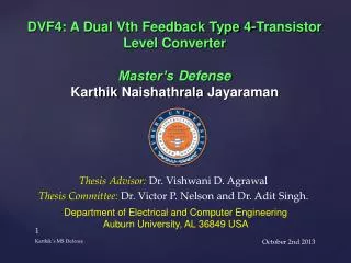
DVF4: A Dual Vth Feedback Type 4-Transistor Level Converter Master’s DefenseKarthikNaishathralaJayaraman • Thesis Advisor: Dr. Vishwani D. Agrawal • Thesis Committee:Dr. Victor P. Nelson and Dr. Adit Singh. Department of Electrical and Computer Engineering Auburn University, AL 36849 USA Karthik’s MS Defense
Problem Statement • Motivation • Introduction and Background • Types of Level Converters • Level Converters • Proposed Level Converter • Design of Level Converter • Experimental Results • Conclusion Presentation Outline Karthik’s MS Defense
To design a level converter which has less power consumption and reduced delay. • The average power and delay of one standard inverter as a target for the level converter. • To have a better energy saving by allowing the level converters overhead than energy saving obtained by using Dual-VDD design without allowing level converters. Problem Statement Karthik’s MS Defense
Problem statement • Motivation • Introduction and Background • Types of Level Converters • Level Converters • Proposed Level Converter • Design of Level Converter • Experimental Results • Conclusion Presentation Outline Karthik’s MS Defense
Sun Surface Motivation Source: Patrick P. Gelsinger , Keynote, ISSCC, Feb. 2001 Karthik’s MS Defense
Scaling of device features not only increases the performance of the devices, but also increases the leakage power. This is shown in the Figure below. Motivation Continued.. 180nm 90nm 45nm 32nm Karthik’s MS Defense
Problem Statement • Motivation • Introduction and Background • Types of Level Converters • Level Converters • Proposed Level Converter • Design of Level Converter • Experimental Results • Conclusion Presentation Outline Karthik’s MS Defense
Voltage scaling technique causes the reduction in supply voltage. This reduction causes a quadratic reduction in dynamic power. Leakage power also reduces since the gate leakage. • Dual VDD design technique exploits this concept in causing the reduction in power consumption. • Reduction in VDD causes the degrading in performance of the circuits. • In-order to maintain the performance in dual VDD designs, cells along the critical paths are assigned to be higher supply (VDDH). The cells along the non-critical paths are assigned to the lower power supply (VDDL). Introduction and Background Karthik’s MS Defense
The assigning of low voltage gates is based on two major algorithms • Clustered Voltage Scaling (CVS) • Extended Clustered Voltage Scaling (ECVS). • CVS: The cells driven by each power supply are grouped (clustered) together and level conversion is needed only at sequential elemental outputs. • ECVS: The cell assignment is flexible, allowing level conversion anywhere (not just at the sequential element outputs) in the circuit. • In case of Dual VDD designs level converters may be used to convert the low supply voltage to high supply voltage, to eliminate the undesirable static current that will flow when VDDL gates might feed the VDDH gates. Introduction and Background Continued.. Karthik’s MS Defense
Introduction and Background Continued.. Ref. K. Usami and M. Horowitz, “Clustered Voltage Scaling Technique for Low-Power Design," in Proceedings of the International Symposium on Low Power Design, pp. 23-26, 1995. Ref. K. Usami,et al.,“Automated Low-Power Technique Exploiting Multiple Supply Voltages Applied to a Media Processor," IEEE Journal of Solid-State Circuits, vol. 33, no. 3, pp. 463-472, Mar. 1998. VDDH Level Converter VDDL Karthik’s MS Defense
Problem Statement • Motivation • Introduction and Background • Types of Level Converters • Level Converters • Proposed Level Converter • Design of Level Converter • Experimental Results • Conclusion Presentation Outline Karthik’s MS Defense
Level converters are of two types • Feedback based level converter • Differential cascaded voltage switched (standard level converter) • Pass transistor level converter. • Contention mitigated level converter • Multi-Vth based level converter • Dual Vth cascaded inverter level converter. • Multi- Vth level converter Types of Level Converters Karthik’s MS Defense
Problem Statement • Motivation • Introduction and Background • Types of Level Converters • Level Converters • Proposed Level Converter • Design of Level Converter • Experimental Results • Conclusion Presentation Outline Karthik’s MS Defense
Level conversion (from VDDL to VDDH) becomes essential at boundaries where VDDL driven cell drives a VDDH supplied cell to eliminate the undesirable static current that will otherwise flow. • This current flows, since the logic “HIGH” signal of the VDDL driven cell, cannot completely turn off the pMOS pull-up network of the following VDDH cell. • We will describe some of the various published level converters ranging from standard level converter to the recently published best level converter. Level Converters Karthik’s MS Defense
Standard Level Converter [Masaki et al., 97 ] Pass Transistor Level Converter [M. Hamada, 98] The pass transistor level converter depends on feedback and Dual Vth technique.The star in the transistor denotes the low-Vthdevices. This level converter consumes less energy than the DCVS level converter due to its fewer devices and reduced contention. The standard level converter which (Differential cascade voltage switched) depends upon feedback circuitry. This converter consumes significant energy due to the contention at the points of connection of the cross- coupled pair and the pull-down nMOSnetwork. Level Converters Continued.. Karthik’s MS Defense
Conventional Type II [Wang, 01] Contention Mitigated [Sakurai, 05] Conventional Type II converters when compared to cross-coupled level-shifter this shows better performance in operating speed, within same size. To operate at low core voltage, the low to high level shifting M1and M2 need to be changed to thin gate-oxide transistor. Contention Mitigated has a small delay. The power consumption of the CMLS is reduced because the contention reduction also brings in the crowbar current reduction, , but its power is relatively large because of stacked pMOS transistors Level Converters Continued.. Karthik’s MS Defense
Dual Vth Cascaded Inverter [Tawfik, 07] Multi- Vth Level Converter [Tawfik, 07] Multi-Vthlevel converter. M2 has higher Vthin order to eliminate the static DC current when the input is low (IN_VDDL). The speed is enhanced due to the shorter input-to-output signal propagation path and the elimination of the contention current during the output low-to-high transition. The level converter is composed of two dual-Vth cascaded inverters. The Vth of M2 is high for avoiding static DC current in the first inverter, when the input is at VDDL. It has fewer transistors compared to the level converters discussed together causing the reduction in power consumption. Level Converters Continued…. Karthik’s MS Defense
The level converters are simulated using 32nm PTM technology model in HSPICE. The simulation setup is shown in the figure. • The power consumption and the delay values are tabulated. The delay values are the average of rise and fall delay. Simulation setup Karthik’s MS Defense
Average power in µW, VDDH = 1.0V. Karthik’s MS Defense
Average Power (µW) V/S VDDL (V) Karthik’s MS Defense
Delay Values in ps , VDDH = 1.0V Karthik’s MS Defense
Delay (ps) versus VDDL(V) Karthik’s MS Defense
Problem Statement • Motivation • Introduction and Background • Types of Level Converters • Level Converters • Proposed Level Converter • Design of Level Converter • Experimental Results • Conclusion Presentation Outline Karthik’s MS Defense
DVF4: A Dual Vth Feedback Based 4-Transistor Level Converter Karthik’s MS Defense
In this work we propose a new level converter based on feedback technique and multi- Vthtechnique. “DVF4: Dual Vth Feedback based 4 Transistor Level Converter”. • DVF4 is composed of four pass transistors. The threshold voltage of M3 and M4 transistors are high to avoid the static DC current. • We have M4 transistor as a feedback circuitry which is needed to pull-down to logic ‘0’ when there is a ‘0’ at the input. DVF4: A Dual Vth Feedback based 4-Transistor Level Converter Continued… Karthik’s MS Defense
Problem Statement • Motivation • Introduction and Background • Types of Level Converters • Level Converters • Proposed Level Converter • Design of Level Converter • Experimental Results • Conclusion Presentation Outline Karthik’s MS Defense
The working of the level converter is as follows. • When there is VDDL on the input, M2 is ON forcing the drain of M2 to be `0'. This turns M3 ON, the output node goes to High (Logic `1'). A logic `1' on the output keeps M4 OFF making no change to the gate of M3. we have a stable `1'. • Now, when we have a logic `0' at the input of the Level Converter, the `0' is passed by the M1, since, M1 is always ON. A `0' at the output turns M4 ON, keeping the gate of M3 to be `1', so that M3 is OFF, providing a proper `0' at the input. If M4 is absent, then the gate of M3 will be at a intermediate voltage caused by the previous logic state, so we do not have a proper `0' at the output. Design of Level Converter DVF4 Level Converter Karthik’s MS Defense
The level converter is optimized using an optimizing program written in PERL for power consumption and delay, by changing the widths of transistors M3 and M4, and threshold voltages of M3 and M4 individually for each VDDL. • After the optimization is done the width of the M4 transistor was found to be approximately constant at 0.110u. • The level converters are simulated using 32nm PTM technology model in HSPICE. 100 vectors with the interval of critical delay is applied at the input • A load of inverter which is four times the standard inverter is connected at the output as simulation setup. The power consumption and the delay values are tabulated. Design of Level Converter Karthik’s MS Defense
Power, Delay of DVF4 V/S Input Voltage (VDDL) Karthik’s MS Defense
Problem Statement • Motivation • Introduction and Background • Types of Level Converters • Level Converters • Proposed Level Converter • Design of Level Converter • Experimental Results • Conclusion Presentation Outline Karthik’s MS Defense
The DVF4 level converter is compared with the previous best level converter. The simulation setup is depicted below. • The first inverter supplied by VDDL and the second inverter connected after the Level converter is supplied by VDDH. • The driver and load inverters are 4X the size of a minimum size inverter (Wn = 4Wmin and Wp = 10Wmin). • The simulations are done using the 32nm PTM model in HSPICE. Experimental Results Karthik’s MS Defense
Comparison of DVF4 v/s Multi Vth Level Converter Karthik’s MS Defense
Average power of DVF4 V/S Multi Vth Level Converter Karthik’s MS Defense
Delay of DVF4 V/S Multi Vth Level Converter Karthik’s MS Defense
In this section we utilize the algorithm 4 for assigning Level Converter and algorithm 2 from Allani to find the optimum voltage (VL) for various benchmark circuits. • We then use the DVF4 level converter for High to Low conversion in the places assigned by algorithm 4. • For simulations for ISCAS’85 Benchmark circuits we use 90nm PTM model in HSPICE. 100 random vectors at a period of the critical path were used for the simulations. • The motivation is to have better savings in energy by allowing level converters than by using only Dual VDD. Dual Voltage and Level Converter Assignment Karthik’s MS Defense
Dual Voltage Assignment with Level Converters Karthik’s MS Defense
In order to determine whether the level converter can be used to reduce the power consumption in case of Dual VDD design and still maintain the critical delay of the circuit, we utilize the inverter tree circuit. • We can determine how many gates can be assigned VDDL and find the optimum low voltage (VDDL) at which the critical path delay can be maintained and still save the power consumption. • We then compare DVF4 with Multi Vth level converter. In order to determine the critical delay, an inverter tree is first simulated with VDD. Inverter Tree Combination Karthik’s MS Defense
The inverter tree is simulated for 100 cycles of toggling inputs with 100 vectors with critical delay as the period for each input vector. • The simulations are done using 32nm predictive technology model. • The power and delay values are calculated using HSPICE. The power savings is 0 in this case if level converters are not allowed . Inverter Tree Combination Setup & Results Karthik’s MS Defense
When the inverter tree chain is simulated with DVF4 level converter. The simulations are done using the voltage supplies as shown in the Figure. The number of VDDL gates is 6 and number of VDDH gates is 2. • The power values are obtained using HSPICE. The number of VDDL gates is determined by the critical delay found without level converters Inverter Tree Combination Results Karthik’s MS Defense
When the inverter tree chain is simulated with previous best Existing level converter. The simulations are done using the voltage supplies as shown in the Figure. The number of VDDL gates is 4 and number of VDDH gates is 4. • The power values are obtained using HSPICE. The number of VDDL gates is determined by the critical delay found without level converters. Inverter Tree Combination Results Karthik’s MS Defense
Inverter Chain Comparison of DVF4 and Multi VthLevel Converter, VDDH =1.0V Karthik’s MS Defense
Problem Statement • Motivation • Introduction and Background • Types of Level Converters • Level Converters • Proposed Level Converter • Design of Level Converter • Experimental Results • Conclusion Presentation Outline Karthik’s MS Defense
The DVF4 level converter was compared to the multi-Vth level converter (best existing level converter) using various simulation setups and the results were obtained for different voltage supplies for multi-V DD systems. • The circuits were optimized and simulated at 32nm CMOS technology, the proposed level converters offer us a significant savings on power consumption of up to 58% and the delay savings up to 77%. • This level converter could be used and can produce lower power consumption in spite of the overhead, based on the data obtained from the simulations as discussed in this work. Conclusion Karthik’s MS Defense
M. Allani, “Polynomial-Time Algorithms for Designing Dual-Voltage Energy Efficient Circuits,” Master's thesis, Auburn University, Auburn, Alabama, Dec. 2011. • M. Allani and V. D. Agrawal, “Energy-EcientDual-Voltage Design Using Topological Constraints,” J. Low Power Electronics, vol. 9, no. 3, pp. 275-287, Oct. 2013. • A. P. Chandrakasan and R. W. Brodersen, Low Power Digital CMOS Design,Springer, 1995. • S. H. Kulkarni and D. Sylvester, “High Performance Level Conversion for Dual VDD Design,” IEEE Trans. VLSI Systems, vol. 12, no. 9, Sept. 2004. • S. H. Kulkarni, A. N. Srivastava, and D. Sylvester, “A New Algorithm for Improved VDD Assignment in Low Power Dual VDD Systems," in Proc. International Symp. Low Power Design, 2004, pp. 200-205. • S. H. Kulkarni and D. Sylvester, “Fast and Energy Efficient Asynchronous Level Converters for Multi-VDD Design [CMOS ICs]," in Proc. IEEE International System on Chip Conf. • M. Kumar, S. K. Arya, and S. Pandey, “Level Shifter Design for Low Power Applications,“ International Journal of Computer Science and Information Technology, vol. 2, no. 5, Oct. 2010. References Karthik’s MS Defense
S. Narendra and A. Chandrakasan, Leakage in Nanometer CMOS Technologies, Springer, 2006. • B. C. Paul, A. Agarwal, and K. Roy, “Low-Power Design Techniques for Scaled Technologies,” Integration, the VLSI Journal, vol. 39, no. 2, pp. 64-89, 2006. • M. Pedram and J. M. Rabaey, “Power Aware Design Methodologies”. Springer, 2002. • J. Rabaey, Low Power Design Essentials,Springer, 2009. • J. Rabaey, A. P. Chandrakasan, and B. Nikolic, Digital Integrated Circuit - A Design Perspective,Pearson Education, 2003. • S. A. Tawk and V. Kursun, “Multi-VthLevel Conversion Circuits for Multi-VDD Systems,” in Proc. International Symp. Circuits and Systems, May 2007, pp. 1397-1400. • K. Usami and M. Horowitz, “Clustered Voltage Scaling Technique for Low-Power Design," in Proc. International Symp. Low Power Electronics and Design, 1995, pp. 3-8. • K. Usami, M. Igarashi, F. Minami, T. Ishikawa, M. Kanzawa, M. Ichida, and K. Nogami, “Automated Low-Power Technique Exploiting Multiple Supply Voltages Applied to a Media Processor," IEEE Journal of Solid-State Circuits, vol. 33, no. 3, pp. 463-472, Mar. 1998. References Karthik’s MS Defense
THANK YOU!!!! Karthik’s MS Defense