Download
1 / 15
150 likes | 281 Vues
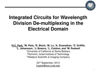
Integrated Circuits for Wavelength Division De-multiplexing in the Electrical Domain. 1 H.C. Park, 1 M . Piels , 2 E. Bloch, 1 M. Lu, 1 A. Sivanathan , 3 Z. Griffith, 1 L . Johansson, 1 J . Bowers, 1 L . Coldren , and 1 M . Rodwell

E N D
Integrated Circuits for Wavelength Division De-multiplexing in the Electrical Domain 1H.C. Park,1M. Piels, 2E. Bloch,1M. Lu,1A. Sivanathan, 3Z. Griffith, 1L. Johansson, 1J. Bowers, 1L. Coldren, and 1M. Rodwell 1University of California at Santa Barbara 2Technion, Israel Institute of Technology 3Teledyne Scientific & Imaging Company 23rd September, 2013 hcpark@ece.ucsb.edu 1
Outline • Motivation • New Proposed WDM Receivers • Test Setups and Results • Two channel (SSB rejection) tests • Three channel (adjacent channel rejection) tests • Conclusion 2
Motivation • Network Traffics / High Data Rate Demands • More bandwidth • Higher spectral efficiency • Low power consumption • System complexity and cost • Long reach • Toward 1Tb/s using a Single Receiver (System) • System Directions: • Coherent (phase/amplitude) modulations (i.e. 16QAM) • Dual polarizations • Gridless channels • Super-channels • Photonic and electronic Integrations • Low power / high efficiency High Speed Systems High Efficiency Systems 3
Conventional WDM Receivers • Configuration: Photonic IC + Electrical IC • WDM multi-channels • De-multiplexing using AWG • Integrated LO lasers • 90° optical hybrids • Balanced photo-diodes (PDs) • EIC: TIAs + filters + ADCs + DSPs Photonic IC • Complex PIC • Large die: expensive • Many interfaces between PIC & EIC • Fixed WDM channel spacing 4
Proposed WDM Receivers • Single-chip Multi-channel WDM Receivers: Toward 1Tb/s • Simple PIC: one LO + one optical hybrid + one set of PDs • Complex EIC • TIAs + filters + ADCs + DSPs • SSB mixers • Electrical LOs • Challenges: high speed PDs1) and high speed EIC2) References: 1) >300GHz PDs – Ishibashi et. al. 2) 1THz TRs – Jain Vibhor et. al. EIC • One set of interface between PIC & EIC • Flexible WDM channel spacing • Complex EIC: OK!! • Small and simple PIC 5
Two-Stage Down-conversion: Optical, then Electrical 1) Optical LO for optical down conversion for all WDM channels Optical WDM channels become subcarriers in the electrical domain 2) Electrical LO for selected channel with SSB mixers Selected channel down-converted to near DC 3) Other channels removed by filtering Then, ADC + DSP DATA recovery 6
System Demonstration using OMA+EIC (2-channels) Real-time oscilloscope OMA* as PICs Free space optics 90° optical hybrid & Balanced PDs OMA* blocks As PICs 2-channel electrical IC *OMA – optical modulation analyzer • Ref. Agilent N4391A Optical Modulation Analyzer Measure with confidence • http://cp.literature.agilent.com/litweb/pdf/5990-3509EN.pdf 7
Two-channel Tests: Single-side-band Suppression (+/- channels) I & Q outputs (+) channel (-) channel Activated channel Suppressed channel 8
Two-channel Tests: Single-side-band Suppression • EIC outputs (Electrical Spectrum Analyzer) 9 • About 25dB SSB suppression • Negligible channel interference • x2 more channels within the PDs and EIC bandwidth
Three-channel Tests: Adjacent Channel Rejections (+/- channels) I & Q outputs 10GHz Spacing 5GHz Spacing (no guard band) 20GHz Spacing Tested with different channel spacing !! 10 *Measured spectrums by an optical spectrum analyzer
Three-channel Tests: Adjacent Channel Rejections • Eye Qualities with Different Filter Combinations BER 1.0E-9 *Filter1: before optical modulators to suppress the side lobes *Filter2: after EIC outputs to filter out the other channels 11
Future Tests: 6-channel WDM Receivers • Concept schematics (PIC + EIC) • EIC for 6-channel receivers is ready to test ! 12
Future Tests: 6-channel WDM Receivers • 6-channel WDM receiver IC • Teledyne 500 nm InP HBT: ~300GHz ft, fmax • 1st design spin: no attempt to design for low power • Simulations (5Gb/s BPSK) • 30Gb/s for BPSK, 60Gb/s for QPSK, 120Gb/s for 16QAM are feasible! • 6-channel initial EIC only tests (done) • 6-channel system demonstrations will be done (soon)! 4.8 x 1.5 mm2 ±12.5GHz ±62.5GHz ±37.5GHz I-output Q-output I-output Q-output I-output Q-output 13
Conclusion • The first concept demonstration using two channel EIC receivers • Spectral efficiency is maximized using a minimum channel spacing • 5Gb/s using two channel receivers • Using 8-channels / 25GHz spacing / 100GHz EIC / 100GHz PDs / PDM • 0.8Tb/s for QPSK, 1.6Tb/s for 16QAM • 5GHz spacing data recovery • Flexible channel (<10GHz) designs • Future Works • 6-channel demonstration soon • PIC + EIC demonstration soon • Silicon based designs in near future • Low power consumption • Small IC size 14
Thanks for your attention! Questions? hcpark@ece.ucsb.edu 15