Best Practices for ESD Component Placement in PCB Design
Proper placement of ESD (Electrostatic Discharge) components is critical in PCB design to enhance protection and minimize damage risks. This guideline emphasizes the importance of reducing inductance by positioning the TVS (Transient Voltage Suppressor) diode close to the I/O line. Avoiding sharp bends and keeping solder pads in proximity to their respective components significantly decreases the clamping voltage experienced by integrated circuits during ESD events. Implementing these layout considerations can lead to effective ESD protection and improved circuit reliability.

Best Practices for ESD Component Placement in PCB Design
E N D
Presentation Transcript
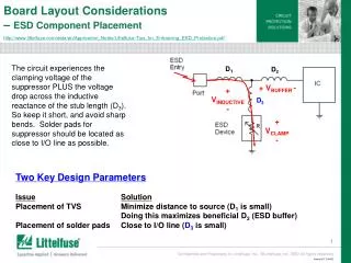
Board Layout Considerations– ESD Component Placement http://www.littelfuse.com/data/en/Application_Notes/Littelfuse-Tips_for_Enhancing_ESD_Protection.pdf The circuit experiences the clamping voltage of the suppressor PLUS the voltage drop across the inductive reactance of the stub length (D3). So keep it short, and avoid sharp bends. Solder pads for suppressor should be located as close to I/O line as possible. D1 D2 + VBUFFER - + VINDUCTIVE - D3 + VCLAMP - Two Key Design Parameters IssueSolution Placement of TVS Minimize distance to source (D1 is small) Doing this maximizes beneficial D2 (ESD buffer) Placement of solder pads Close to I/O line (D3 is small)
Board Layout Considerations– ESD Component Placement (cont) Effects of Poor Layout: Let’s assume the board designer adds a stub trace (i.e. D3) to connect the ESD device and puts it very close to the IC. Given typical PCB materials, the resulting inductances could be: D1=2nH, D2~0nH, D3=2nH. Assume a RDYN=1.0Ω. An 8kV ESD strike is equivalent to a 30A current pulse in 1ns. This will create an additional 60V on top of the clamping voltage of the ESD component and the IC will see a minimum of 90V! D1 D2 + 60V - D3 + 30V - *NOTE: Putting the ESD device closer to the “Port” would make D2 much bigger. Consequently, the non-linearity of inductor D2 would act as a buffer to the initial peak current of the ESD pulse by providing a substantial voltage drop “toward” the IC.