Download
1 / 38
400 likes | 873 Vues
Flash Memory Fault Modeling and Test Algorithm Development. Adviser: Prof. Cheng-Wen Wu 吳誠文 教授 Student: Jen-Chieh Yeh 葉人傑 May 06, 2004. LAB for Reliable Computing Department of Electrical Engineering National Tsing Hua University Hsinchu, Taiwan 30013. Outline. Introduction

E N D
Flash Memory Fault Modeling and Test Algorithm Development Adviser: Prof. Cheng-Wen Wu 吳誠文 教授Student: Jen-Chieh Yeh 葉人傑 May 06, 2004 LAB for Reliable Computing Department of Electrical EngineeringNational Tsing Hua University Hsinchu, Taiwan 30013
Outline • Introduction • Flash Memory Overview • Flash Memory Testing Issues • Flash Disturb Fault Modeling • Flash Test Algorithm Development • Built-In Self-Test (BIST) Design • Experimental Results • Conclusions
Semiconductor Memory Market Forecast of Web Feet Inc.
Introduction • Flash memories are becoming widely used in many applications • High density, Low power,On-line update, Non-volatile … • Embedded Flash coresthus play an important role in the System-on-Chip (SoC) environment MP3 player MD DSC Cell-phone
Flash Memory Applications NAND SSD USB Drive Serial Access MCP PDA DSC NOR G3 Phone MP3 Cell Phone DVD STB Industrial Controls Random Access PC BISO Low Density High Density Note: MCP = NOR or NAND based Flash devices including RAM in a Multi Chip Package
Two Major Architectures of Flash B$ Forecast of Web Feet Inc.
NAND and NOR Architectures Bit-line Word-line Source line NAND NOR
Read Operation V>0 ID “0” “1” GND GND Vread ID(“1”) VT GND Decoder SA ID(“0”) VT_Erase Vread VT_Program VGS “0” or ”1”
Write Mechanism Program Operation (μs) Erase Operation (m s) Vwl>>0 Vwl<<0 GND Vs>0 Vbl>0 Vbl>0 Vbody>0 Channel Hot Electron (CHE)injection in the floating gate atthe drain side Fowler-Nordheim (FN)electron tunneling current throughthe tunnel oxide from the floatinggate to the silicon surface Erasure is usually performed over a complete block or chip, and hence the name “Flash” Different process technologies and even manufactures may differ in their choice of the program/erase mechanism
Flash Memory Testing Issues • Reliability issues • Disturbances: inadvertent change of the cell content due to reading or programming another cell • Over-erasing: overstressed cell after erase, leading to unreliable program operation • Endurance: capability of maintaining the stored information within specified operation count • Retention: capability of maintaining the stored information within specified time limit • Long program/erase time • Difficult test access for embedded Flash memory • ATE price is high, and grows rapidly
Growth of Embedded Flash Memory Embedded Flash Memory Shipments(Worldwide, $ Millions) $ 600 $ 500 $ 400 $ 300 $ 200 $ 100 2000 2001 $ 0 2002 2003 2004 2005 Forecast of CISG (Cahners In-Stat Group)
Approaches • Reasonable fault models for reliability-related defects • Efficient test algorithms to reduce test time and increase fault coverage • Built-in self-test (BIST) circuit for embedded Flash memories • Replace or reduce the requirement of ATE • “Built-in self-test and built-in self-repair will be essential to test embedded Flash memories and to maintain production throughput and yield.”[Quoted ITRS 2003]
Contribution to Flash Memory Testing Study of Flash Memories Flash Disturb Fault Modeling Fault Simulator:RAMSES-FT Test Algorithm Development Test Algorithm Generation by Simulation: TAGS Proposed First Built-In Self-Test Design for Flash Complete Experimental Results
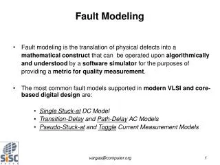
Fault Modeling • Fault model is defined faulty cell behavior • Fault model makes analysis possible • Fault model makes effectiveness testing • Fault model limits the scope of test pattern Defects in Layout Defects in Transistor Faulty Cell Behavior Fault Model
Flash Memory Specific Faults • IEEE Standard 1005, “Definitions and Characterization of Floating Gate Semiconductor Arrays”, defines the disturbance conditions • Flash memory functional fault models • Word-line Program Disturbance (WPD) • Word-line Erase Disturbance (WED) • Bit-line Program Disturbance (BPD) • Bit-line Erase Disturbance (BED) • Over Erasing (OE) • Read Disturbance (RD) ProgramDisturb Fault Erase Disturb Fault Read Disturb Fault
Program Disturb Faults • Word-line Program Disturbance (WPD) • A cell transits from 1 to 0 when another in the same word-line is being programmed (1 to 0) • Word-line Erase Disturbance (WED) • A cell transits from 0 to 1 when another in the same word-line is being programmed (1 to 0) • Bit-line Program Disturbance (BPD) • A cell transits from 1 to 0 when another in the same bit-line is being programmed (1 to 0) • Bit-line Erase Disturbance (BED) • A cell transits from 0 to 1 when another in the same bit-line is being programmed (1 to 0)
Word-line Program Disturbance • WPD Conditions: 1.Victim cell initial value is a logic ‘1’ 2.Aggressor “10” (program) Victim “10” (program) G Control Gate S D Floating Gate V(L) V(H) Source Drain V(H) Substrate V(L) B V(Gd)
Word-line Erase Disturbance • WED Conditions: 1.Victim cell initial value is a logic ‘0’ 2.Aggressor “10” (program) Victim “01” (erase) G Control Gate S D Floating Gate V(L) V(H) Source Drain V(H) Substrate V(L) B V(Gd)
Bit-line Erase Disturbance • BED Conditions: 1.Victim cell initial value is a logic ‘0’ 2.Aggressor “10” (program) Victim “01” (erase) G Control Gate S D Floating Gate V(L) V(H) Source Drain V(H) Substrate V(L) B V(Gd)
Bit-line Program Disturbance • BPD Conditions: 1.Victim cell initial value is a logic ‘1’ 2.Aggressor “10” (program) Victim “10” (program) V(H) During programming, erased cells on unselected rows on a bit-line that is being programmed may have a fairly deep depletion region formed under them Electrons entering this depletion region can be accelerated by the electric field and injected over the oxide potential barrier to adjacent floating gates V(H) V(L) V(Gd)
Read Disturbance and Over Erase • RD • A cell transits from 0 to 1 during the read cycles • Relationship with read count (n) • <Rn0, 1> • In here, we assumed n = 1 • OE • The threshold voltage of a cell is low enough to turn the cell into a depletion-mode transistor • Cell can not be programmed correctly • Reading a cell on the same bit line induces a leakage current, resulting in an erroneous read
Conventional RAM Faults • Several conventional RAM fault models are also considered useful for testing Flash memory • Stuck-At Fault (SAF) • Cell or line sticks at 0 or 1 • Transition Fault (TF) • Cell fails to transit from 0 to 1 or 1 to 0 • Stuck-Open Fault (SOF) • Cell not accessible due to broken line • State Coupling Fault (CFst) • Coupled cell is forced to 0 or 1 if coupling cell is in given state • Address-Decoder Fault (AF) • A functional fault in the address decoder
Test Algorithm Development • for the sake of fault coverage (FC) • March algorithm often applies test to the SRAM and DRAM • Ex: {(w0);(r0,w1,r1);} bit-oriented • Ex: 0000 {(wa); (ra); (wb); (rb);} word-oriented Fault Model Test Algorithm Built-In Self-Test Built-In Self-Repair Tester
Bit-oriented Flash Memory Test • Conventional March tests can not detect all Flash specific faults • No (w1) operation in Flash technology • ProposedMarch Flash Test (March-FT) • {(f );Ý(r1,p0,r0); (r0); (f ); ß(r1,p0,r0); (r0);} • Regular, easier to generate, covering more functional faults and do not rely on the array geometry or layout topology
Word-oriented Flash Memory Test • Word-oriented memory may have intra-word faults • Add simple test with multiple standard backgrounds to cover intra-word faults • {(f );(pa,ra); (f ); (pb,rb);} • Number of backgrounds is log2(m)+1 • m : word width • 1 : solid background • Example (m = 4): 0000(f );Ý(rb,pa,ra); (ra); (f ); ß(rb,pa,ra); (ra); 0011 (f );(pa,ra); (f ); (pb,rb);0101 (f );(pa,ra); (f ); (pb,rb); “0000” is solid background “0011” & “0101” are standard backgrounds
Flash Memory Fault Simulator • RAMSES-FT • Detect all base fault & disturb fault • Used scaling technique • Support word-oriented Flash • Support physic-address for disturb fault
March-FT Simulation Result • {(f); (r1,p0,r0); (r0); (f); (r1,p0,r0); (r0)}
Simulation Results • Bit-oriented Flash memory tests simulation result(128Kbits Flash memory) Assumption: F=190ms, P=8us, R=50ns, and N=128K
Simulation Results (cont.) • Word-oriented Flash memory tests simulation result(128Kx4bits Flash memory, word width: 4) Assumption: F=190ms, P=8us, R=50ns, and N=128K
Test Algorithm Generation by Simulation • TAGS [VTS2000]
BIST Advantages • Functional test (Go / No go) • Tester functional easily (Few Logic I/O) • Test throughput increased (Pin Count Reduction) • Test program simply (Engineer Mode) • System-on-Chip (SoC) testing easily Normal Mode Signal Flash core Go/NoGo BIST BNS MUX BMS CLK
Built-In Self-Test Design • Flash memory BIST block diagram BSI: BIST serial input BSO: BIST serial output BMS: BIST mode selectBRS: BIST reset BNS: BIST/Normal select BCE: BIST commend endCLK: System clock
Case I • A typical 4Mbits (512K x 8) embedded Flash memory core with BIST circuitry
Case II • A commodity 1Mbits (128K x 8) Flash memory chip with BIST circuitry
Conclusions • Bit-oriented and word-oriented Flash memory tests are proposed • Implemented the BIST circuit for the embedded Flash memory core and commodity Flash memory chip • A Flash memory simulator has been developed to facilitate the analysis and generation of the tests • Developed March-like test methodology that can be used and reused for various Flash memories • Our future work is to support more Flash memory types and other realistic fault models, and to develop a diagnosis and repair methodology for Flash memories