Download
1 / 39
400 likes | 616 Vues
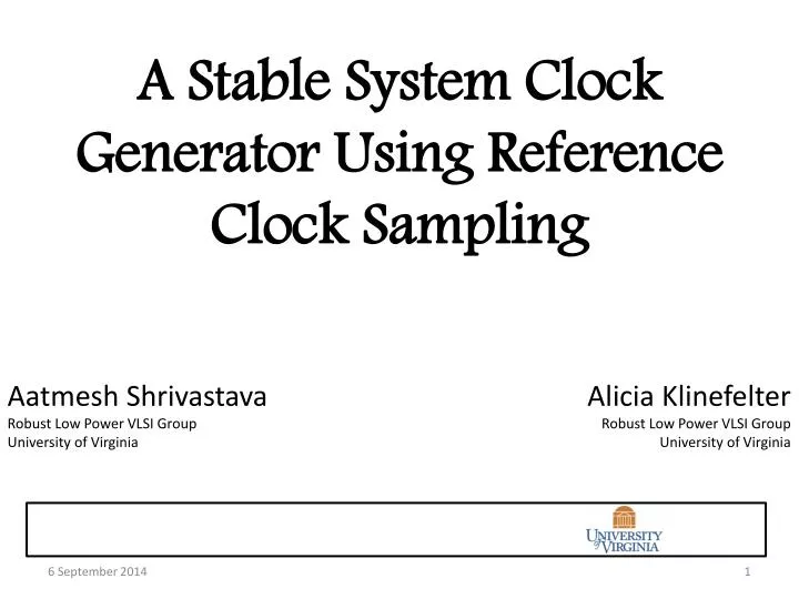
A Stable System Clock Generator Using Reference Clock Sampling. Aatmesh Shrivastava Robust Low Power VLSI Group University of Virginia. Alicia Klinefelter Robust Low Power VLSI Group University of Virginia. Outline. Motivation Crystal oscillator design and power consumption

E N D
A Stable System Clock Generator Using Reference Clock Sampling AatmeshShrivastava Robust Low Power VLSI Group University of Virginia Alicia Klinefelter Robust Low Power VLSI Group University of Virginia
Outline • Motivation • Crystal oscillator design and power consumption • Novel Circuit Architecture • Three phases of operation viz calibration, conversion and retention phase • Circuit Design: Calibration Phase • F to V converter • Op-Amp • VCO • PTAT • Conversion and Retention Phase • ADC • Capacitive DAC • R-2R DAC • Summary • References
Motivation : Crystal Oscillator CRYSTAL • Almost all microprocessors, micro-controllers, PICs, and CPUs operate using a crystal oscillator. • Crystal oscillator provides the reference clock. • Why?? • Highest accuracy and frequency stability compared to any known oscillator. • Usually Fed to PLL to generate system clock, Sometimes can be used as is. • Frequency range from 10Khz-50Mhz CRYSTAL SYMBOL Equivalent circuit Circuit Diagram of Xtal oscillator Board Hook-up
Motivation : Crystal Oscillator Power • Crystal with Char. frequency of 32Khz to 50Mhz designed to obtain power. • Most optimal point for oscillation. • Crystal parameter obtained through vendor data-sheets. • Power dissipated ranges from 2.6uW @ 32Khz to 70mW @ 50Mhz. • At 200Khz power ranges from 5uW to 30uW. • Crystal Oscillator consumes significant amount of power, critically impacts the power consumption of a system designed for lower power.
Motivation : Proposed Circuit technique • We propose a fully integrated reference/system clock circuit in CMOS. • The circuit achieves a high frequency stability of +/-250ppm. • We reduce the power consumption to a very low level < 2u Watts @ 200Khz • Unlike a crystal oscillator the power consumption of proposed circuit does not scale up with the frequency because of the architecture. Proposed Circuit
Circuit Operate in 3 Phases. • Calibration Phase. (done=0) • A stable voltage is obtained at A, corresponding to reference frequency through crystal oscillator • The amplifier controls the VCO. The VCO oscillation frequency is converted back to voltage using F to V converter. • Feedback structure makes sure that A=E. (Need very high gain amplifier to insure this) • Calibration is completed once voltage at E becomes equal to A. A E • Conversion Phase. (done=0) • Once E settles to value of A, Analog to Digital converter (ADC) and Digital to Analog Converter is enabled. • These two blocks generates C which is equal to B with <1mV quantization error. • Done signal goes high after conversion is done which causes MUX to select the DAC output. • Retention Phase.(done=1) • After done goes high, DAC is calibrated with desired o/p voltage for VCO. Clock can be turned off. • The voltage at DAC can be maintained through bank of registers. • All other blocks except DAC, PTAT and VCO can be disabled and are disabled. • PTAT controls the temperature drift of VCO.
Circuit Design: Frequency to Voltage converter[1] VDD Is Clk T1 MP1 MN1 Clk T2 T1 T2 C2 C1 MN2 T1 T2 Circuit Diagram FVC • Figure shows Frequency to Voltage converter (FVC) schematic which is based on switching capacitors and current source. • F1 and F2 are pulse signals. • F1 is generated after rising edge of Clock, while F2 is generated after falling edge of F1
Functioning T1 T2 • When Clock is Low MP1 is on transmission gate T1 is off and MN2 is off. • C1 gets charged through Is. Is C1=C2 • When F1 goes high MP1 is off and MN2 is OFF. T1 is on and C1 and C2 Share charge as shown C2 C1 C2 • When F2 goes high T1 is off MP1 is off and MN2 is ON which discharges C1 to ground. • This process is repeated and eventually charges C2 to the maximum Voltage of C1. • A voltage thus inversely proportional to frequency is obtained at C2.
Output waveforms A OUT Steady state internal net waveforms Out build-Up
Circuit Design: Folded Cascode Operational Amplifier VDD VDD + OUT _ INN INP MP2 MP1 VDD VM Cp C OUT VDD M1 A B VM • Gain of the amplifier gets multiplied through each stage. • Very High gain. • Quiescent current = 200nA • Since Op-amp is used in feedback structure, stability of the system is achieved Cp. Compensating Cap MN1 MN2 VM=VDD/2
Stability of the system Feedback path Proposed Circuit Because of the feedback, stability sims were done.
Insuring Stability of the system Pole to replace VCO and F to V for stability analysis REF _ REF OUT _ A A OUT VCO F to V + + = open-loop ac analysis reduction for the system. Feedback portion of the system • As voltage at A changes, frequency of VCO changes and because frequency changes voltage at OUT will changes. In other words voltage at A changes voltage at OUT. • This means there is a phase difference b/w A and OUT or there is a pole b/w A and OUT. • OUT being feedback net so this pole impacts the stability. • We obtain the delay from A to OUT. Using the delay number we approximate the pole by RC and perform open loop AC analysis.
Stability Analysis Phase Margin= DC Gain= 100 dB
Voltage Controlled Oscillator VP VP = IN MP VN _ OUT1 OUT5 BUF INV + VN OPAMP MN Current Mirror Delay Element in VCO • Functioning • Current sources MP and MN determine the delay and hence frequency of VCO. • As Output of OPAMP increases, VN increases and VP decreases. • Current sources MP and MN drive increases, which increases frequency. • Five such delay elements are used.
Voltage Controlled Oscillator Voltage Controlled Oscillator VCO output at VN=700mV VCO output at VN=883mV f=200Khz
Effect of Temperature variation on VCO • After the calibration phase, VCO input would remain at constant voltage. • Temperature will cause current source to vary. • This will change the frequency. • Frequency changes from 220Khz to 200 Khz from 0 to 100oC Sweeping temperature for IN. • With increasing temperature IDRIVE of NMOS drops
Removing effect of Temperature: PTAT[2] • Idrive reduces with temp. Use PTAT to control temperature drift. • Add current of MOS and PTAT to get zero temperature coefficient. (ZTC) • As Temperature increases, the Threshold voltage of transistor decreases. MP1 MP2 IB IB 1 1 • Current in the circuit is given by Start-up MN1 MN2 1 M>1 • With temperature VT of MN1 drops hence VGS, consequently VB increases increasing IB. VGS VB RB
PTAT Output Sweeping temperature for IPTAT.
Getting ZTC currents for VCO Variation of Current sources in VCO. • Current in VCO’s current source vary by 3nA over ~400nA over a temperature variation of 0 to 100oC
VCO output at 0, 50 and 100 Degrees • With change is temperature frequency of oscillation changes from 200 Khz to 201 Khz. • Frequency stability = +/-250ppm
FV1 VCO_in Putting it together: Calibration Phase FV2 VCO_in FV1 FV2 FV2=FV1
Putting it together: Calibration Phase CLKIN VCO_OUT
Successive Approximation (SAR) ADC • Begins by making assumptions about bit values starting with the MSB and forcing 1000…00 (Vref/2)onto the DAC. • If this voltage is above the analog input, the assumed bit goes to 0, else it remains 1. • Then assumptions are made about all bits till the LSB and checked so the system “zeros in” on the result.
SAR ADC Block Diagram [4] • Comparator: Compares assumption coming from DAC and input analog voltage. • DAC: Takes current assumption bits and turns them into analog voltage for comparison in next stage. • SAR Logic: Takes output of comparator (0 or 1) to determine the next bit value and set the next bit assumption.
Comparator • Three op amps used (two P, one N)
The Charge Scaling 10-bit DAC [3] • Capacitor DAC acts as both DAC and sample-hold circuit. • Design consideration: base cap size, C. • Needs to be reset before use (discharge caps).
DAC makes series of guesses. • If (guess voltage) > (analog input) over-approximation. This bit is 0. • Else the guess is below the expected value. This bit is 1.
The R-2R 10-bit DAC [3] • Simple voltage divider network. • Does not require initialization signal and does not need to be periodically refreshed. • Tradeoff: branch current vs. resistor size
The ADC/DAC Network • Active Power consumption: 550nA • Technology: IBM 130nm • Supply Voltage: 1 V • Sampling Rate: 20 kHz • Future optimizations: • Low-power optimization for ADC
Summary • Novel low power, high stability clock circuit is proposed. • The circuit achieves a frequency stability of +/-250ppm. • Power in calibration-phase = 5uW, retention-phase = 2uW. • Similar to crystal in stability (+/-100ppm) better than crystal in terms of power consumption. • Power consumption does not scale up with frequency unlike crystal oscillator
References [1] A Djemouaiet al. “New Frequency Locked Loop based CMOS frequency to voltage converter: Design and Implementation” IEEE Transactions on Circuits and systme II: Analog and Digital Signal Processing. vol. 48 No-5, May 2001. [2] D. Liu et al. “A simple voltage reference circuit using transistor with ZTC point and PTAT current source” IEEE J Solid-State Circuits vol. 29 pp 663- 670, June 1994. [3] Allen E. and Holberg D. “CMOS Analog Circuit Design” Oxford University Press, New York, 2002. [4] Simone Gambini and Jan Rabaey. “Low-Power Succesive Approximation Converter with 0.5 V Supply in 90 nm CMOS” IEE Transactions of Solid-State Circuits. Vol. 42, no. 11, Nov. 2007. Aatmesh as4xz@virginia.edu
BACK UP Aaatmesh
Crystal Oscillator: Design • During start-up phase RBIAS( extremely high value) keeps the Inverter at VM. • Oscillation builds up with noise. • The crystal passes only the resonant frequency voltage, which gets amplifier. • The amplified value gets passed through crystal which again gets amplified. • This goes on till Oscillation saturates. RBIAS CL CL Aatmesh as4xz@virginia.edu
Pole to replace VCO and F to V for stability analysis REF _ REF A OUT _ VCO F to V OUT A + + = Feedback portion of the system Configuration for open-loop ac analysis of the system. A to OUT delay = 100uS So if R=10K C=100pF We choose R=50K and C=100pF for our ac analysis Aaatmesh
Addressing variability: Global variation • Global variation will cause the shift in the current in PTAT which can cause the temperature compensation to drift either in CTAT or PTAT direction. MP1 MP2 IB 1 1 Start-up • Vary RB through bit control to affect a good ztc point. MN1 MN2 1 M>1 RB
Addressing variability: Local Mismatch • Local mismatch can cause an offset which can cause frequency of VCO to be different from Clock. FV1 FV2 • If we bit control the current source of FV2, we can set f(Clock)=f(VCO).
Solution for high frequency clocks • In order to get higher frequency output divide the VCO output by K just like a PLL. • This would have very little impact on over all power consumption of the system.